
Audio-Frequency Doubler
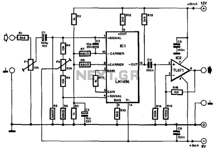
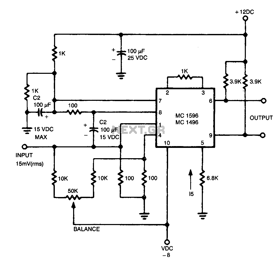
The LM1496 is a versatile integrated circuit designed for frequency modulation and demodulation applications. It is particularly effective in applications where signal integrity and purity are paramount. The circuit's design is predicated on the mathematical relationships between sinusoidal signals, leveraging the chip's ability to double frequencies through the multiplication of two identical frequency signals.
The potential divider at the input serves a dual purpose: it protects the LM1496 from excessive input voltages and ensures that the input signal remains within the operational limits of the chip, thus preserving signal quality. The subsequent amplification stage using an operational amplifier (op-amp) allows for flexibility in output signal levels, making the circuit adaptable to various applications where output strength is critical.
The choice of resistor values for the feedback network of the op-amp is crucial for maintaining the desired gain while minimizing noise. The specified resistor values provide a balance that is essential for maintaining the integrity of the signal throughout the amplification process.
The phase relationship between the input and output signals is a significant consideration in applications involving modulation, as it can affect the overall performance of the system. The ability to suppress the fundamental frequency using a spectrum analyzer illustrates the circuit’s capability to handle complex signal scenarios, making it suitable for advanced communication systems.
The distortion characteristics of the output signal are important for evaluating the circuit's performance in real-world applications. The noted distortion levels at varying input signal strengths indicate the operational limits of the LM1496 and highlight the need for careful signal management in high-frequency applications.
In summary, the LM1496-based circuit provides a robust solution for frequency doubling while maintaining signal integrity. Its design considerations, including input protection, amplification, and distortion management, make it a valuable component in electronic signal processing applications. Often the frequency of a signal must be doubled: modulator/demodulator chip LM1496 is an ideal basis for this. From trigonometry it is well known that: 2simrcosx=sin2* and: sin2 = l-*cos2*. These equations indicate that the product of two pure sinusoidal signals of the same frequency is one signal of double that frequency. The purity of the original signals is important: composite signals would give rise to all sorts of undesired products.
The LM1496 can only process signals that are not greater than 25 mV: above that level, serious distortion will occur. The design is therefore provided with a potential divider at its input. This addition makes it possible, for instance, to arrange for a 500-mV input signal to result in a signal of only 25 mV at the input of the LM1496.
To provide a sufficiently high output signal, the output of IC1 is magnified by op amp IC2, which is connected as a noninverting amplifier. Because the output of IC1 contains a dc component of about 8 V, the coupling between the two stages must be via a capacitor, C4.
With values of R15 and R16 as shown, IC2 gives an amplification of 16 (24 dB). The overall amplification of the circuit depends on the level of the input signal: with an input of 1.2 V, the amplification is unity; when the input drops to 0.1 V, the amplification is just 0.1. The value of the input resistors has been fixed at 680 : this value gives a reasonable compromise between the requirements for a high input impedance and a low noise level.
lb ensure good suppression of the input signal at the output, the voltages at pin 1 and pin 4 of ICl must be absolutely identical to P4, It is possible, With the aid of a spectrum analyzer, to suppress the fundamental (input) frequency by 60 to 70 dB. The output signal at pin 12 is distorted easily, because the IC is not really designed for this kind of operation.
The distortion depends on the level of the input signal. At a frequency of 1 kHz and an input level of 100 mV, the distortion is about 0.6%; when the input level is raised to 500 mV, the distortion increases to 2.3%, and when the input level is 1 V, the distortion is 6%. The signal-to-noise ratio under these conditions varies between 60 and 80 dB. The circuit draws a current of 10 mA from the positive supply line and 5 mA from the negative line. The phase shift between the input and output signals is about 45° (output lags). Finally, although the normal output is taken from pin 12, a similar output that is shifted by 180° (with respect to that at pin 12), is available at pin 6.
🔗 External reference
Related Circuits
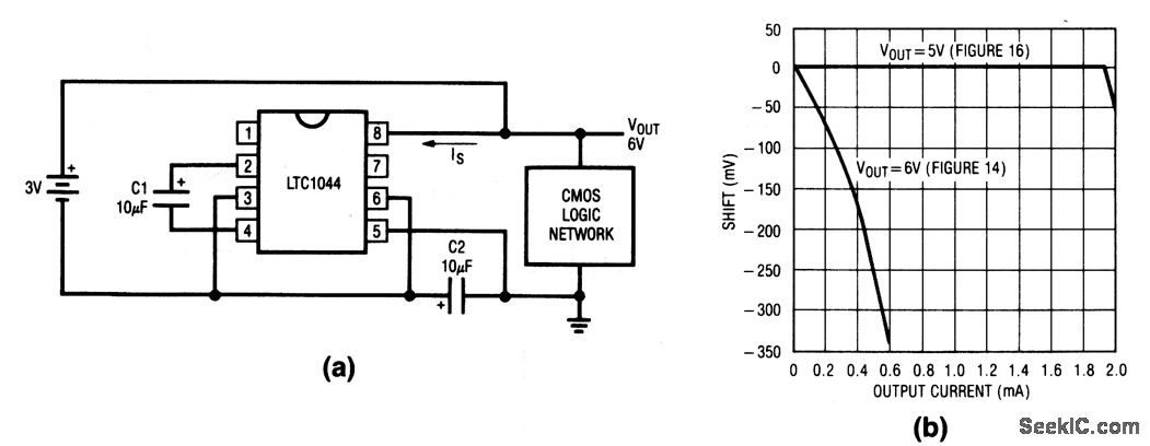
This circuit doubles the available battery voltage using an LTC1044 switched-capacitor voltage converter. It is designed to power low-power 74-CMOS (3 to 15 V) equipment for extended periods from two small 1.5 V cells. The efficiency exceeds 90% for...
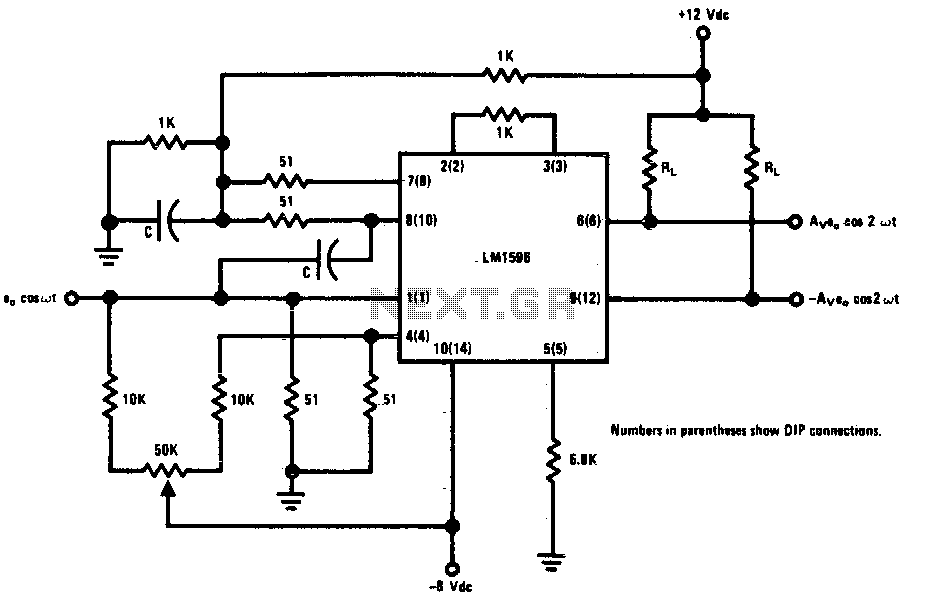
This circuit is designed to double low-level signals while maintaining low distortion. The capacitor value (C) should be selected to ensure low reactance at the operating frequency. The signal level at the carrier input should remain below 25 mV...
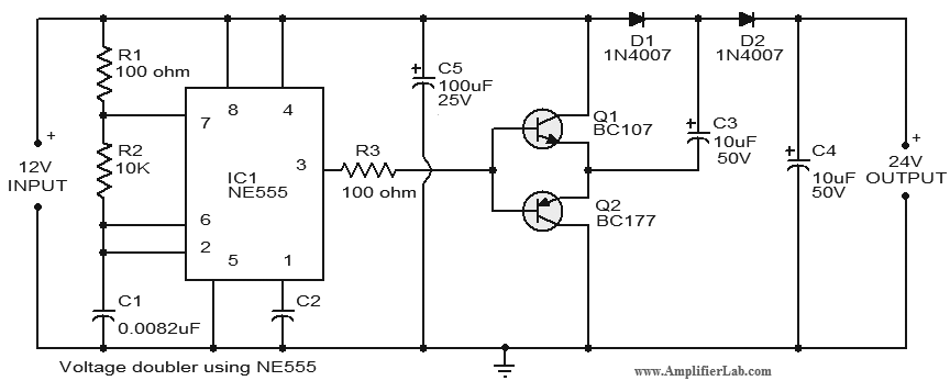
The circuit of the DC Voltage Doubler was designed for a specific type of power supply. It is important to study the schematic design and accompanying photographs of the DC Voltage Doubler circuit to understand the components involved. This...
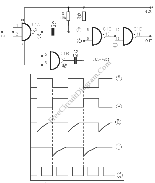
This circuit is a frequency doubler utilizing the 4011 IC. It employs a CMOS quad two-input NAND gate package, specifically the 4011. The circuit consists of two main components. The frequency doubler circuit using the 4011 NAND gate is designed...
The output contains the sum component, which is twice the frequency of the input, since both input signals are of the same frequency. In a circuit design context, the described output suggests the presence of a frequency doubling mechanism, commonly...
Project Manager Jim Heck, G3WGM, has provided an exclusive audio interview to Bob McCreadie, G0FGX, from TX Factor, detailing the tests and potential issues involved. Membership in AMSAT-UK is available to anyone interested in amateur radio satellites or space...