
Frequency Doubler with 4011
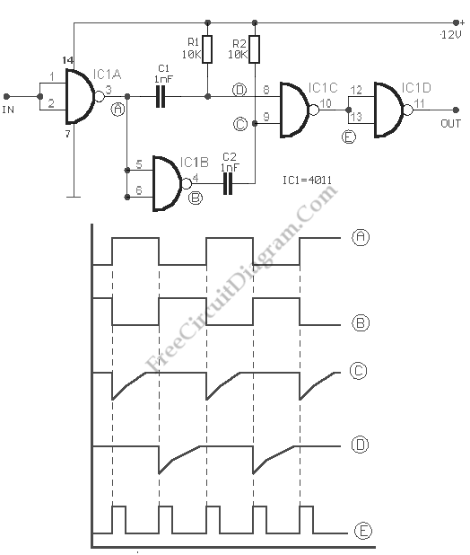
The frequency doubler circuit using the 4011 NAND gate is designed to take an input signal and produce an output signal at double the frequency of the input. The 4011 IC contains four two-input NAND gates, which can be configured to create the desired frequency doubling effect.
To construct the circuit, the first step involves connecting the input signal to the first NAND gate. The output of this gate will be fed into the second NAND gate, which is configured to provide feedback from its output back to one of its inputs. This feedback loop is crucial as it allows the circuit to oscillate, effectively generating a square wave signal at double the frequency of the input.
The operation of the circuit can be understood through the logic states of the NAND gates. When the input signal transitions from low to high, the output of the first NAND gate will switch states, causing the second NAND gate to respond accordingly. The timing of these transitions is such that the output frequency is effectively doubled.
Additionally, appropriate biasing and decoupling capacitors should be included in the circuit design to ensure stable operation and to filter out any noise that may affect the performance of the frequency doubler. The output can be further conditioned with additional circuitry, such as low-pass filters, to smooth out the waveform if necessary.
Overall, this frequency doubler circuit offers a simple yet effective method for generating higher frequency signals using standard CMOS technology. The 4011 NAND gate is a versatile component that provides a reliable solution for various digital applications, including signal processing and communication systems.This is a circuit of Frequency Doubler using 4011. This circuit uses one CMOS quad, two input NAND gate package type 4011. This circuit consist of two. 🔗 External reference
Related Circuits
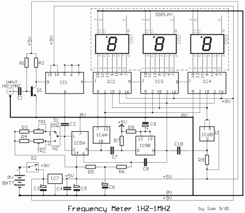
The circuit was designed to create a low-cost frequency meter that will cover the range of 1 Hz to 1 MHz with a digital indication using three 7-segment displays. The frequency meter circuit operates by measuring the frequency of an...
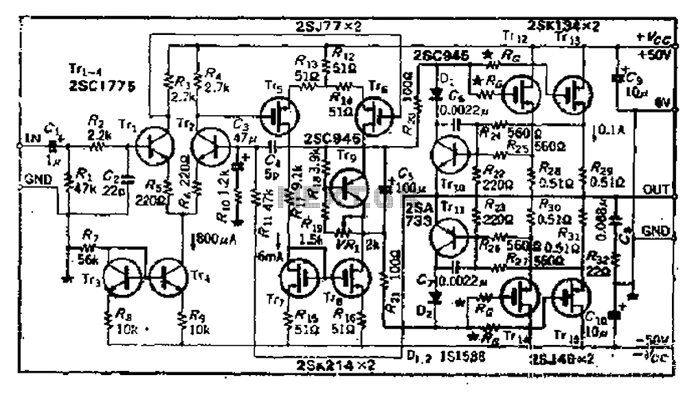
The circuit consists of three identical basic stages, with the second stage featuring a differential output from the power MOSFET, 2SJ77. A current mirror circuit utilizing 2SK214 is implemented. The operating current is 6mA; however, due to the power...
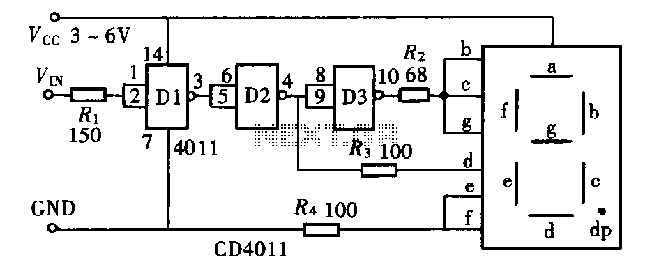
The door circuit logic pen text display can take many forms, utilizing various logic gates such as inverters, NAND gates, NOR gates, and others. A logical pen, exemplified by the NAND gate CD4011, can be used in conjunction with...

The 7208 seven-stage decimal counter can be utilized as a frequency counter. It features latch and multiplexing functions, along with direct digital driving circuitry and display driving circuitry. The output frequency of the 7207 IC 6.5536 MHz crystal oscillator...
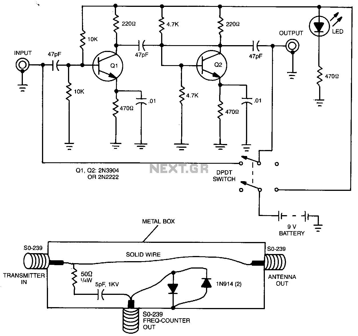
The preamplifier, when utilized with a short length of shielded cable and clip leads, allows signals that typically do not produce a readout to generate precise and stable readings on the counter. A DPDT switch is incorporated to bypass...
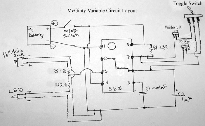
Building your own Zapper. It requires one capacitor of 1 microfarad (C2), preferably unpolarized to eliminate concerns regarding positive and negative terminals. If a polarized capacitor is used, the longer leg indicates the positive side; refer to the schematic...