
Broadband frequency doubler
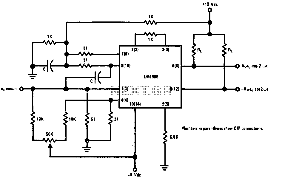
This circuit employs a switching differential amplifier configuration to achieve signal doubling. The amplifier operates in a linear region when the input signal at the carrier input is maintained below 25 mV peak, ensuring minimal distortion in the output. The selection of capacitor C is crucial; it should be chosen based on the operating frequency of the circuit to minimize reactance, thereby optimizing performance.
In scenarios where higher input signals are present, the use of a resistive divider is recommended. This technique allows for the attenuation of the input signal to a level suitable for the carrier input while enabling the full input signal to be utilized at the signal input. The resistive divider should be carefully designed to ensure that the voltage drop across the divider does not exceed the specified threshold for linear operation.
The output waveform integrity is paramount, and while levels approaching 50 mV peak can be accommodated, the resultant distortion must be assessed based on the application's requirements. It is essential to balance the input signal levels and the desired output fidelity to achieve optimal circuit performance.This circuit will double low-level signals with low distortion. The value of C should be chosen for low reactance at the operating frequency. Signal level at the carrier input must be less than 25 mV peak to maintain operation in the linear region of the switching differential amplifier. Levels to 50 mV peak may be used with some distortion of the output waveform If a larger input signal is available, a resistive divider may be used at the carrier input with full signal applied to the signal input. 🔗 External reference
Related Circuits
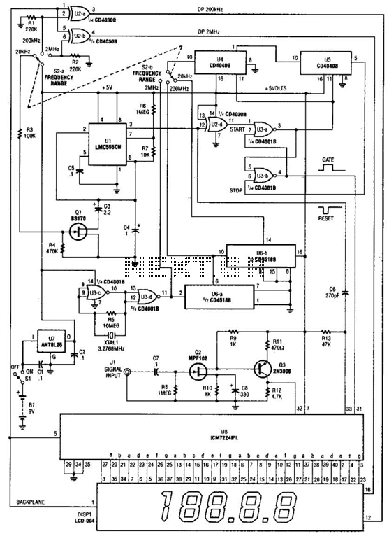
This is a schematic and block diagram of a 2-MHz frequency counter. It utilizes an LSI counter/display driver, an LCD readout, and several logic chips for timebase and timing pulse circuitry. Q2 and Q3 serve as a signal (input)...
The crystal oscillator utilizes two sections of IC1, a 4001 quad 2-input NOR gate, representing a standard and reliable design. The oscillator generates a 1.85-MHz square-wave output that feeds into IC2, a 4017 divide-by-10 counter. The count enable and...
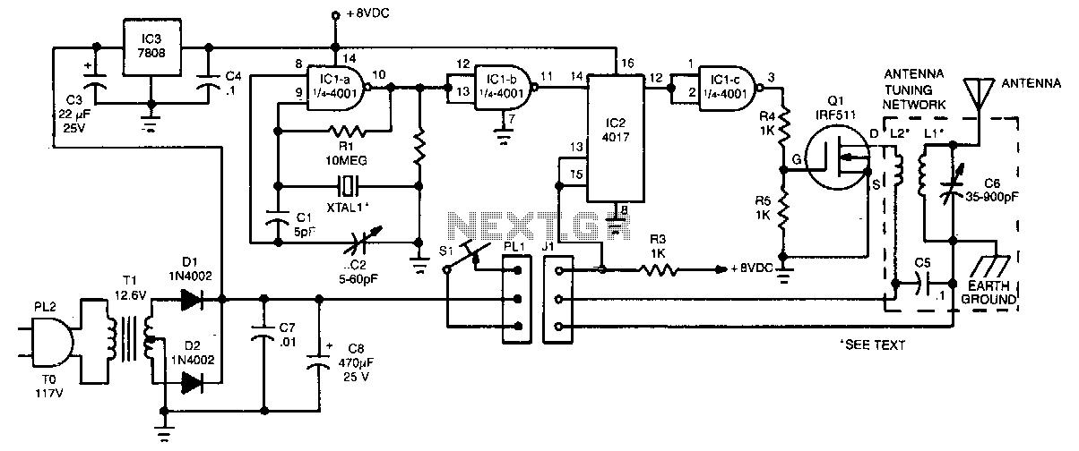
A schematic diagram of the oscillator is presented in Figure 1. The common-base transistor stage (Q1) amplifies the signal within the positive feedback loop. The positive feedback signal develops across the resistor R1, which is shared by the emitters...
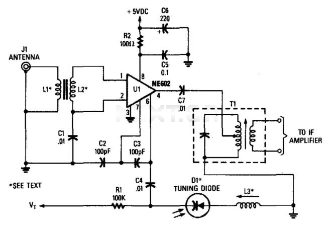
In this configuration, the NE602 serves as a frequency converter in a superheterodyne front-end setup. L1 and L2 form a broadband toroidal transformer, although a tuned transformer may also be utilized. The supply voltage ranges from +5 to +9...
In these applications, a pulse input at a specified percentage is differentiated by a capacitor-resistor (C-R) network. The negative-going edge at pin 6 triggers the input comparator, activating the timer circuit. Similar to a voltage-to-frequency (V-to-F) converter, the average...
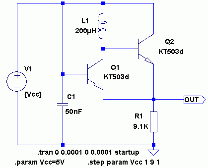
The circuit is a standard RC phase shift oscillator that utilizes a single bipolar transistor as the active component. When power is supplied, regenerative feedback is applied through capacitor C2 from the collector to the base of the transistor....