
AVR ATtiny USB Tutorial
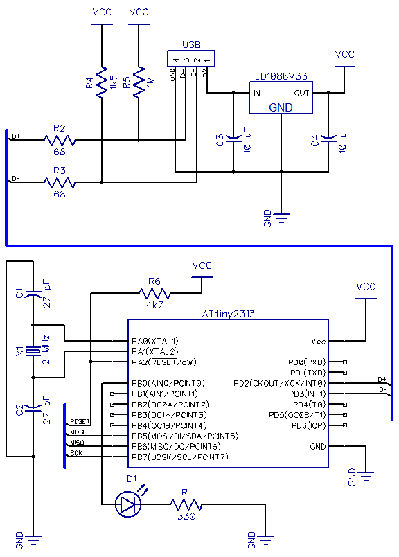
The schematic described involves several critical components and connections essential for the operation of the ATtiny2313 with the V-USB library. The power circuit is a key element, where a voltage regulator is utilized to step down the 5V from the USB to 3.3V, ensuring that the ATtiny2313 operates within its voltage specifications. The D+ and D- lines are equipped with pull-up resistors to ensure proper USB communication, and the use of zener diodes is recommended to protect the ATtiny2313 from voltage spikes.
The ATtiny2313 microcontroller serves as the central processing unit, with its pins configured for USB communication and programming. The RESET pin is connected to a pull-up resistor to ensure that the microcontroller can be reset correctly, while the programming header allows for easy reprogramming and debugging. The addition of a 12 MHz crystal oscillator is crucial for maintaining accurate timing and functionality, particularly when operating at higher frequencies. The ceramic capacitors connected to the crystal are essential for stabilizing the oscillator circuit, which is vital for reliable operation.
Testing the setup with the provided blink program is an effective way to ensure that all connections are functioning correctly. The adjustments to fuse settings allow for configuration of the clock speed, enabling the microcontroller to operate at its optimal frequency. This also provides a practical demonstration of the impact of clock settings on the performance of the LED blinking rate.
Overall, this schematic and setup provide a robust foundation for further development and experimentation with USB applications using the ATtiny2313 and the V-USB library, paving the way for more advanced projects in the future.This is the second part of my USB tutorial for ATtiny2313 and V-USB library. In the first part we learned how to get 3. 3V from USB to power our circuits. In this part, we will expand our setup with following parts: Update: Some people have noted that the setup I`m using here runs ATtiny2313 at 12 MHz with only 3. 3V VCC, which is outside the specif ied range (frequencies over 10 Mhz require 4. 5V or more). I`ve never had any problems, and many others have succeeded with this setup, but if you encounter persistent problems, I suggest you to power the ATtiny2313 straight from 5V of the USB line and use zener diodes on D+ and D- lines to drop their voltage, as is done in my later tutorial with the ATtiny85 microcontroller. This time I will not walk you through every connection. Instead, I`ll just outline the steps needed and show the pictures of end result. Here is the schematic we`re building: Basically it`s the regulator circuit we just built, pullups and line resistors for D+ and D- in the USB bus going to PD2 and PD3, and the ATtiny2313 with RESET pullup and MISO, MOSI, SCK and RESET connected to the 6-pin programming header, and a 12 MHz crystal.
An easy order to make these connections is to: Reconstruct the power circuit from part 1 in one corner of the breadboard. Instead of connecting 5V from USB to the positive power rail, connect it straight to the input pin of the regulator we won`t be needing 5V anywhere else By the way, if you need a refresher on how to connect the RESET pullup and 6-pin header and use the programmer, check out this excellent tutorial wiring is the same but of course pin locations in ATtiny2313 are different than in ATtiny45.
Connecting the crystal is also very easy, just connect the two legs of the crystal to PA0 and PA1, and add ceramic capacitors between each leg and ground (they need to be close to the crystal to make it stable). Now for the good stuff! If you did not already test that your ATtiny2313 setup is working, I suggest you to do that now. A good way to do it is to use the following simple test program: #include
Now for ATtiny2313, we want to disable the internal clock/8 division and use an over 8 MHz clock with 14 clock cycles + 4. 1 ms startup delay (CLKSEL=1111, SUT=10). This means that low fuse should be 0xEF, which is done using avrdude command -U lfuse:w:0xef:m (without quotes).
In case you are using any other part or just want to check it yourself, use the excellent AVR Fuse Calculator. Once you have updated the lfuse, reset or reprogram the chip to verify that the LED is now blinking 12 times per second.
Update the blink example`s F_CPU to 12000000L and reflash to verify that the blinking returns to 1 Hz speed. Congratulations, everything is now ready for the V-USB -part of the tutorial! I will stop here for tonight, and post the third part of this tutorial shortly, covering the basic V-USB setup for our circuit.
🔗 External reference
Related Circuits
This resource contains step-by-step information for creating an AVR microcontroller programmer, complete with a suitable circuit diagram. This programmer is capable of programming 8051, AT89XX, AT90XXXX, and 8031 family microcontrollers. The AVR microcontroller programmer described is designed to facilitate the...
Useful as a transmitter tune-up meter or an RF sniffer, this is an RF field strength indicator that is loosely based on the Broad Band RF Field Strength Probe, described elsewhere. It detects RF via a square law detector,...
This project is designed to charge a pair of AA Nickel Metal Hydride (NiMH) or Nickel Cadmium (NiCd) cells using a laptop's USB port for power. It addresses the need for a convenient charging solution. Any USB port can...
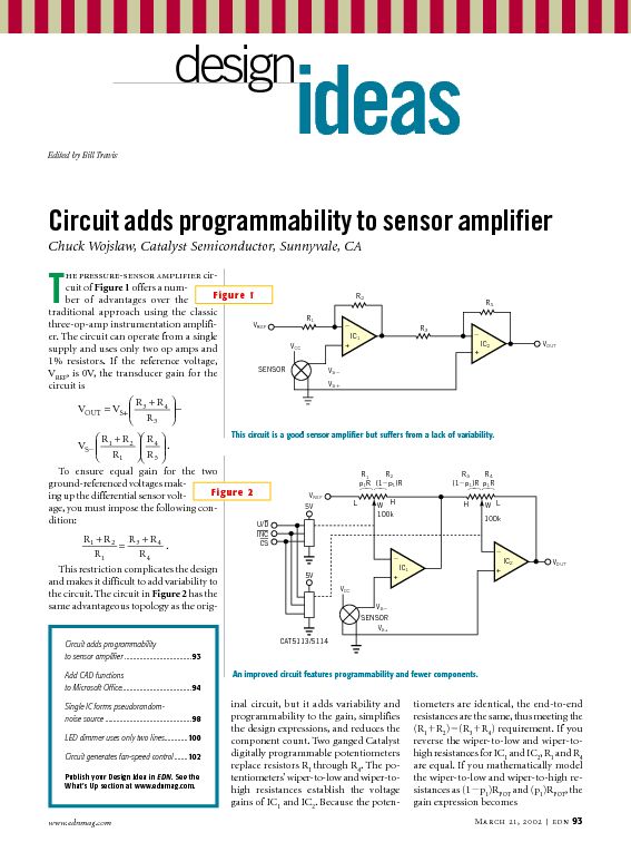
This tutorial provides information related to sensor amplifiers, schematics, and noise. It presents a discussion around sensors and their outputs. Sensor amplifiers are critical components in various electronic systems, especially in applications where signals from sensors need to be conditioned...
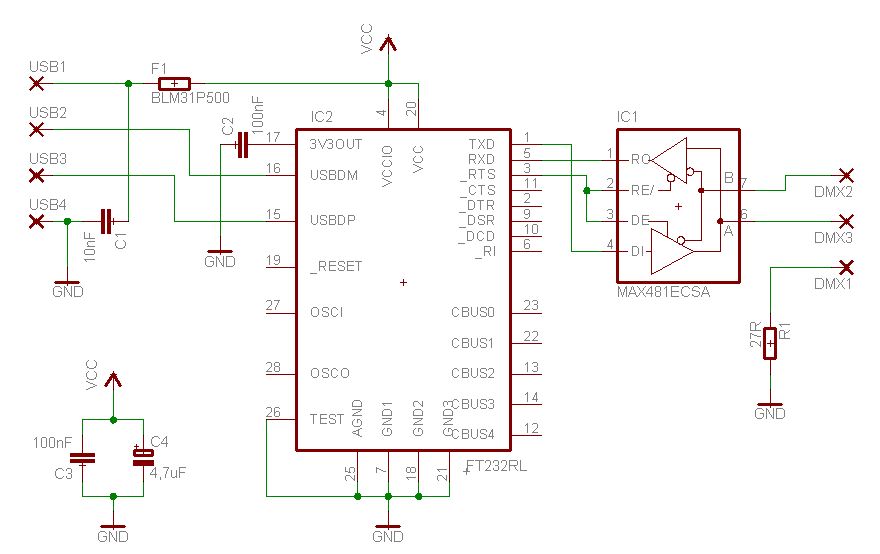
On the DMX line side, an XLR connector should be utilized, either a 3-pin or 5-pin connector. The pins in an XLR connector are typically numbered, eliminating the need for a visual reference. In the case of the 5-pin...
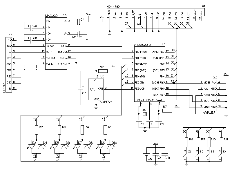
The LCD display is represented by the connector X1. It has a HD44780 compatible LCD controller and is using the 4-bit interface to send data to the LCD controller. The LEDs are multiplexed. It is possible to connect 12...