
Basic gate function
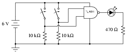
The circuit design centers around a single NAND gate, which is a fundamental component in digital electronics, known for its versatility in creating various logic functions. The 4011 IC contains four independent NAND gates, allowing for multiple configurations within a single package. The circuit is initiated by connecting two input switches to the NAND gate, which serve as the control mechanism for the gate's output state. The LED indicates the output of the NAND gate, providing a visual representation of the logic operation.
In the schematic, the power supply connections are critical for the proper functioning of the NAND gate. The VDD and ground connections must be established accurately to ensure that the gate operates within its specified voltage range. The recommended practice of connecting unused gate inputs to either VDD or ground is essential to prevent floating inputs, which can lead to unpredictable behavior and potential damage to the IC.
The use of an 8-position switch and a 10-segment LED bar graph, while seemingly excessive, allows for greater flexibility in circuit testing and experimentation. This arrangement enables the user to explore various input combinations and observe the corresponding output states on the LED bar graph, thereby enhancing the learning experience.
In summary, careful attention to the connections and configurations within the circuit is paramount. Utilizing the datasheet for the 4011 chip ensures that all pin assignments are correctly implemented, minimizing the risk of errors and promoting a successful circuit assembly. The design emphasizes the importance of grounding unused gates and maintaining a clean layout to facilitate future modifications and expansions.To begin, connect a single NAND gate to two input switches and one LED, as shown. At first, the use of an 8-position switch and a 10-segment LED bargraph may seem excessive, since only two switches and one LED are needed to show the operation of a single NAND gate. However, the presence of those extra switches and LEDs make it very convenient to e xpand the circuit, and help make the circuit layout both clean and compact. It is highly recommended that you have a datasheet for the 4011 chip available when you build your circuit. Don`t just follow the illustration shown above! It is important that you develop the skill of reading datasheets, especially "pinout" diagrams, when connecting IC terminals to other circuit elements.
The datasheet`s connection diagram is an essential piece of information to have. Shown here is my own rendition of what any 4011 datasheet shows: In the breadboard illustration, I`ve shown the circuit built using the lower-left NAND gate: pin #`s 1 and 2 are the inputs, and pin #3 is the output. Pin #`s 14 and 7 conduct DC power to all four gate circuits inside the IC chip, "VDD" representing the positive side of the power supply (+V), and "Gnd" representing the negative side of the power supply (-V), or ground.
Sometimes the negative power supply terminal will be labeled "VSS" instead of "Gnd" on a datasheet, but it means the same thing. Digital logic circuitry does not make use of split power supplies as op-amps do. Like op-amp circuits, though, ground is still the implicit point of reference for all voltage measurements.
If I were to speak of a "high" signal being present on a certain pin of the chip, I would mean that there was full voltage between that pin and the negative side of the power supply (ground). Note how all inputs of the unused gates inside the 4011 chip are connected either to VDD or ground. This is not a mistake, but an act of intentional design. Since the 4011 is a CMOS integrated circuit, and CMOS circuit inputs left unconnected (floating) can assume any voltage level merely from intercepting a static electric charge from a nearby object, leaving inputs floating means that those unused gates may receive any random combinations of "high" and "low" signals.
Why is this undesirable, if we aren`t using those gates Who cares what signals they receive, if we are not doing anything with their outputs The problem is, if static voltage signals appear at the gate inputs that are not fully "high" or fully "low, " the gates` internal transistors may begin to turn on in such a way as to draw excessive current. At worst, this could lead to damage of the chip. At best it means excessive power consumption. It matters little if we choose to connect these unused gate inputs "high" (VDD) or "low" (ground), so long as we connect them to one of those two places.
In the breadboard illustration, I show all the top inputs connected to VDD, and all the bottom inputs (of the unused gates) connected to ground. This was done merely because those power supply rail holes were closer and did not require long jumper wires!
Please note that none of the unused gate outputs have been connected to VDD or ground, and for good reason! If I were to do that, I may be forcing a gate to assume the opposite output state that it`s trying to achieve, which is a complicated way of saying that I would have created a short-circuit.
Imagine a gate that is supposed to output a "high" logic level (for a NAND gate, this would be true if any of its inputs were "low"). If such a gate were to have its output terminal directly connected to ground, it could never reach a "high" state (being made electrically common to ground through the jumper wire connection).
Instead, its upper (P-channel) output transistor would be turned on in vain, sourcing maximum current to a nonexistent load. This would very likely damage the gate! Gate output terminals, by their very nature, generate the 🔗 External reference
Related Circuits
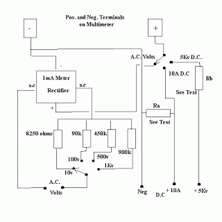
A combination of shunts and multipliers, selected via a switch, can be utilized alongside a single basic meter to create a multirange instrument known as a multimeter. This device is capable of measuring voltage, current, and resistance. A multirange...
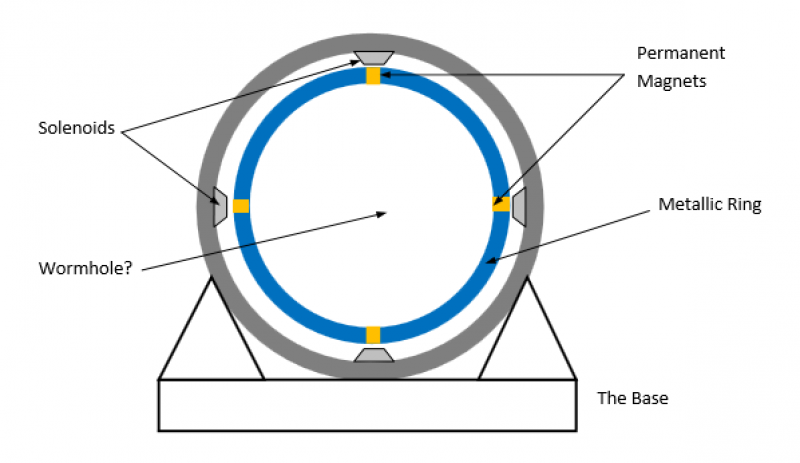
This type of travel may be possible if two space points can be connected by a vortex channel in aether. The channel allows continuity of matter, energy, and life by establishing a connection between two distant points. The vortex...
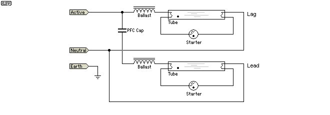
Fluorescent lamps, despite their long presence, remain enigmatic to many individuals due to their complex operational mechanisms. The lamp consists of a gas mixture, primarily containing mercury, which, when energized as an arc, produces a significant amount of short-wave...
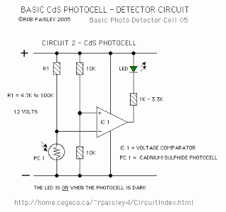
This is a basic Cadmium Sulfide (CdS) photocell detector circuit. In this circuit, when light falling on the photocell (PC1) is blocked, its resistance increases, causing the voltage across PC1 to rise. When the voltage exceeds half of the...
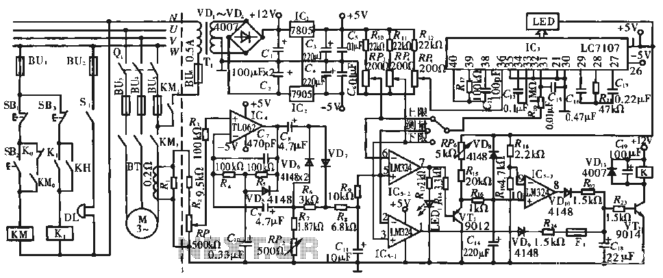
The circuit operates during standard inspection work by utilizing the voltage across resistor R2, which is connected to RP, to generate the input signal for IC4. Components R3 through Rg, along with capacitors C7 and C1, and diodes VD7...
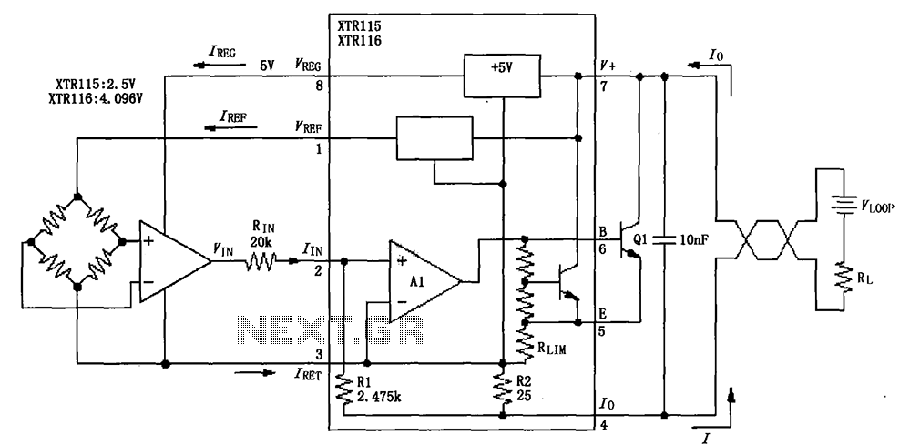
The output reference voltage VREF from the O pin is not utilized within the internal circuit; instead, it is provided to the external circuit. Similarly, the output voltage VREG is also supplied to the external circuit. All current return...
Warning: include(partials/cookie-banner.php): Failed to open stream: Permission denied in /var/www/html/nextgr/view-circuit.php on line 713
Warning: include(): Failed opening 'partials/cookie-banner.php' for inclusion (include_path='.:/usr/share/php') in /var/www/html/nextgr/view-circuit.php on line 713