
XTR115 116 Basic circuit diagram connection
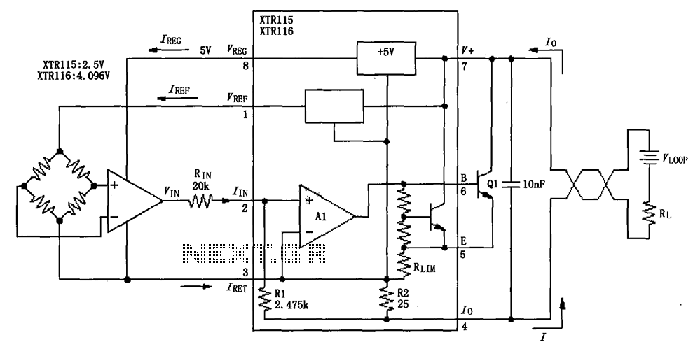
The described circuit configuration features a dual-output system, where VREF and VREG serve as critical voltage references for external applications. The VREF output is designed to provide a stable reference voltage, ensuring that external components can operate reliably without being influenced by internal circuit variations. This design choice enhances the flexibility of the circuit, allowing it to interface seamlessly with a variety of external devices.
The VREG output serves a similar purpose, supplying a regulated voltage to external circuits that may require a specific operating voltage. This output is essential for maintaining consistent performance across different load conditions, thereby improving the overall robustness of the system.
The current return paths, denoted as IRET, are integral to the circuit's functionality. These paths are designed to manage the return current effectively, ensuring that the system remains stable and that the input circuit operates correctly. The IRET configuration is crucial for minimizing noise and interference, which can adversely affect the performance of sensitive electronic components.
The operational specifications indicate that the output current Io can vary between 4 mA and 20 mA, making it suitable for applications such as industrial sensors and actuators that require precise current control. The input current IIN has a range of 40 µA to 200 µA, indicating that the circuit is designed to handle a wide range of input signals while maintaining accuracy and efficiency. The input voltage VIN operates between 0.8 V and 4 V, providing the necessary voltage levels for proper circuit operation.
Overall, this circuit design emphasizes flexibility and stability, making it well-suited for various applications in electronic systems where external interfacing and current regulation are critical. As shown in FIG, O pin output reference voltage VREF is not used for the internal circuit, it is supplied to the external circuit; similarly, pin output voltage VREG is supplie d to the external circuit. And all the current return feet (IRET end), the input circuit is, IRET ends the equivalent of to. Io The circuit is 4 ~ 20mA, IIN is 40 ~ 200 A, VIN is 0.8 ~ 4V.
Related Circuits
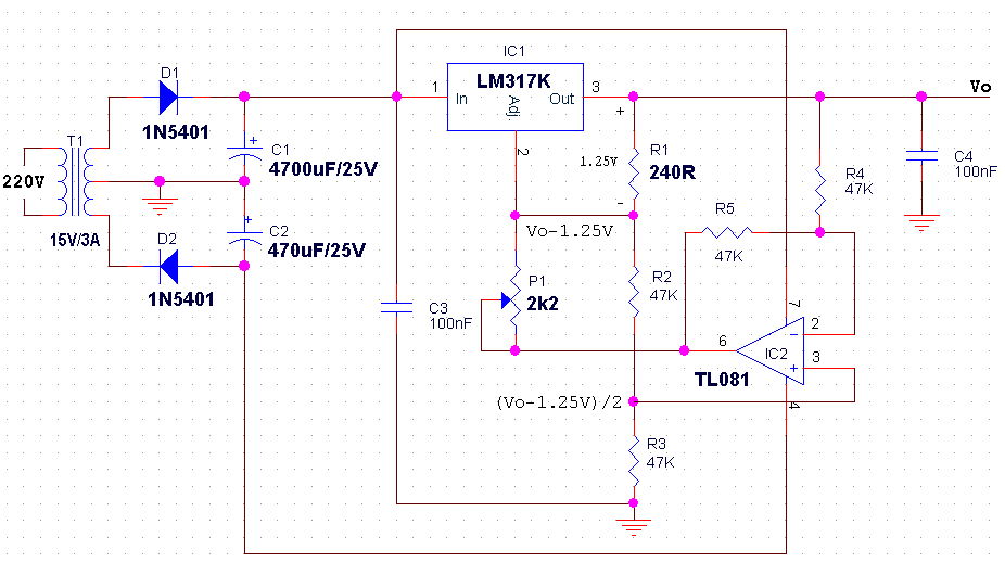
The LM317 is an adjustable, positive 3-terminal voltage regulator capable of supplying 100 mA (for RA87U control) or 1.5 A (for Order Code UF27E and N61CA) across an output voltage range of 1.2 V to 37 V. These voltage...

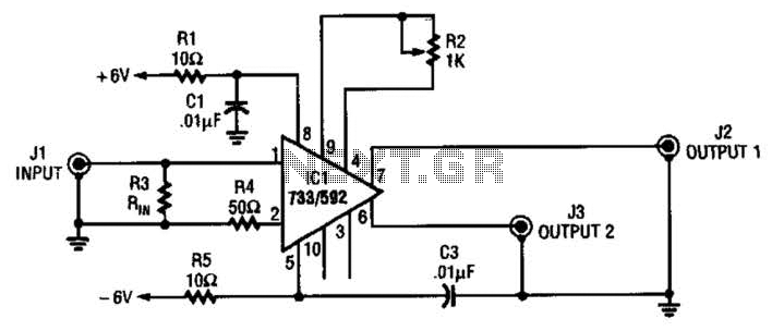
The inverting input is maintained at a low level via a 10K resistor when the circuit is powered on but not in use. During measurement activities, including calibration measurements where the input is floating, this resistor is disconnected. The...
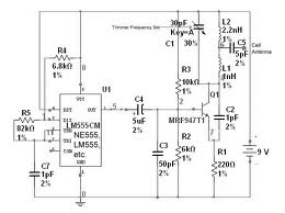
The team is highly interested in the design of a jammer circuit and has begun working on it. However, they are experiencing issues with the circuit, specifically that the signal is not being jammed effectively. The design of a jammer...
This circuit selects one of two channels using a logic signal. The unused channel is shorted out to minimize crosstalk. The bandwidth at -3 dB is approximately 8 MHz. It is recommended to buffer this circuit due to some...
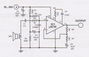
This microphone preamplifier utilizes the low-noise integrated circuit (IC) uA739. The circuit serves as an example of an effective design for preamplifying dynamic microphones. The IC contains two operational amplifiers. The uA739 is a precision integrated circuit known for its...
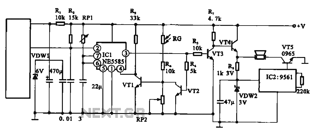
This circuit illustrates an automatic unattended burglar alarm system designed primarily for residential use, warehouses, and similar applications. The circuit features a pyroelectric infrared sensor integrated with a light control mechanism. It comprises components such as resistors (RG, RP2,...
Warning: include(partials/cookie-banner.php): Failed to open stream: Permission denied in /var/www/html/nextgr/view-circuit.php on line 713
Warning: include(): Failed opening 'partials/cookie-banner.php' for inclusion (include_path='.:/usr/share/php') in /var/www/html/nextgr/view-circuit.php on line 713