
Blochead Diamond Buffer
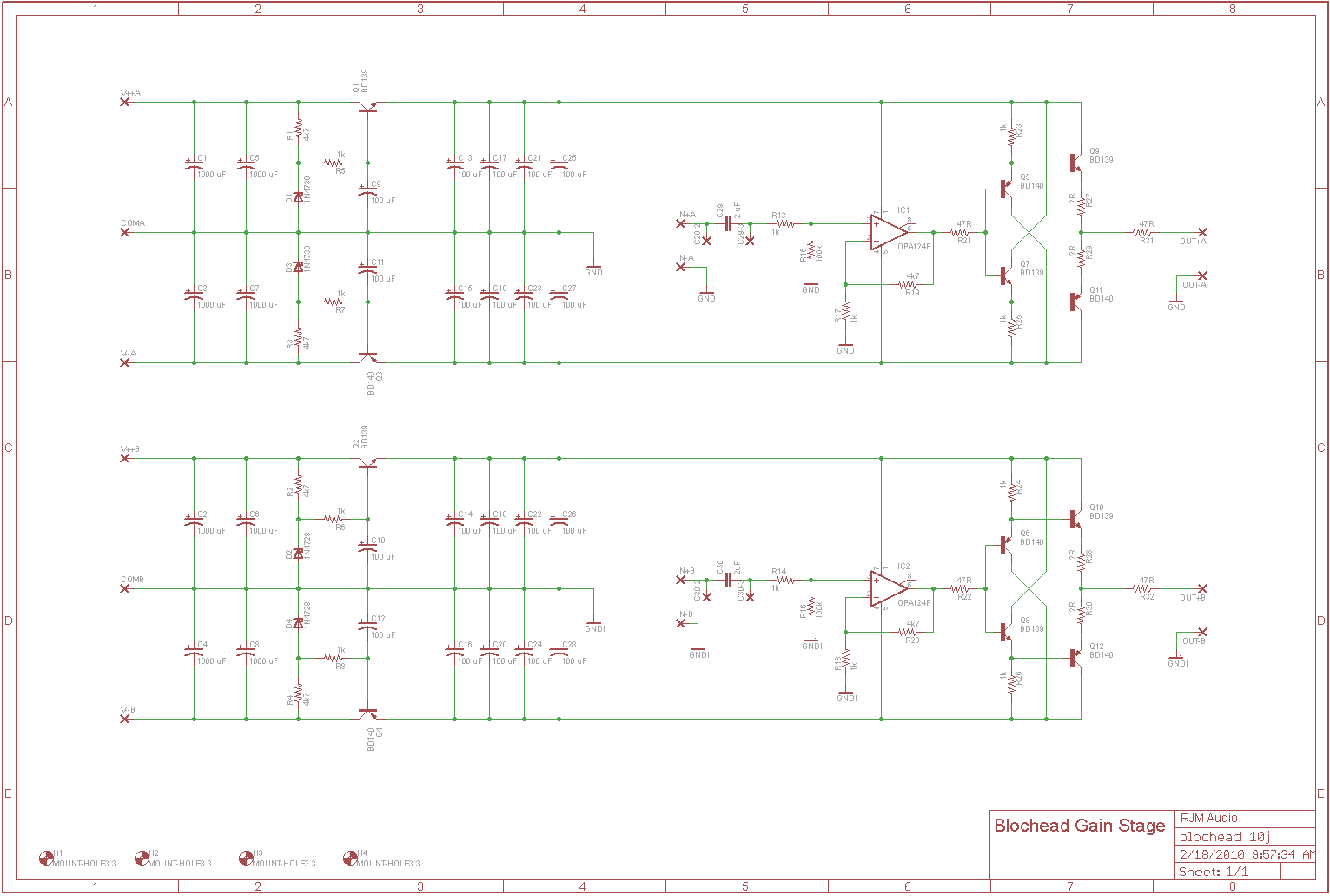
The described circuit employs a 100k volume potentiometer, serving as the input stage for either line-level signals or headphone outputs. The non-inverting gain stage provides an amplification of 15 dB, which is suitable for boosting low-level audio signals to a more manageable level before further processing. This gain stage is critical in ensuring that the subsequent buffer stage receives a strong enough signal to maintain fidelity and performance.
The buffer stage, based on a discrete configuration of the LH0002, utilizes four transistors that are meticulously matched. This matching is essential for ensuring low output offset voltage, which is crucial in audio applications where even minor voltage offsets can lead to audible distortion or imbalance in sound reproduction. The design's decision to avoid including the buffer in the feedback loop of the operational amplifier is a notable aspect, as it allows for a more straightforward circuit design while still achieving desired performance metrics.
However, the buffer's architecture presents certain inefficiencies. The need for the driver transistors to draw the same amount of current as the output devices leads to a significant increase in overall current consumption—about three times that of a more conventional design. This elevated current demand can be a drawback in terms of power efficiency, particularly in battery-operated applications.
The use of very small damping resistors on the output emitters is a critical design consideration. These resistors serve to stabilize the output stage and maintain linearity. If the resistors are too large, the output stage may not pull static current effectively, leading to a transition to Class B operation, which can introduce distortion and reduce sound quality. The minimalist approach taken in this design emphasizes simplicity and efficiency, aiming to deliver high-quality audio performance while minimizing components and complexity.
Overall, this circuit exemplifies a thoughtful balance between performance and simplicity, making it suitable for both line-level and headphone applications while addressing key challenges in audio amplification design.The circuit is designed to run off a 100k volume pot, and be either a line stage or a headphone amplifier. It is a standard non-inverting gain stage (A=15dB) followed by discrete copy of the old LH0002 buffer IC.
The basic idea is that the four transistors in the buffer will be carefully matched to ensure low output offset voltages and low distortion, so that it will not be necessary to include it in the op amp feedback loop. The rather primitive buffer is inefficient as the driver transistors must pull as much current as the output devices, so the total current is about 3x more. It also means the damping resistors on the output emitters can only be very tiny otherwise the output stage pulls no static current and reverts to class B operation.
I am drawn to the minimalist design however. 🔗 External reference
Related Circuits
This simple amplifier is ideal for adding a headphone jack to equipment that lacks this feature. The Headphone Buffer circuit board is small enough (1.2" X 1.4") to squeeze into even the smallest spaces and power requirements are so...
Prior to the test point, there is an AD744 operational amplifier with its output connected to a 10nF capacitor. Following this, a 1kΩ resistor connects to ground. From the junction where the capacitor and resistor meet, a 4.7kΩ resistor...
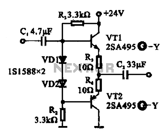
A buffer amplifier is utilized as a transistor emitter follower buffer amplifier for applications that necessitate a high input impedance. The circuit employs a complementary push-pull configuration. The signal input is connected to the base of transistor VT1, which...
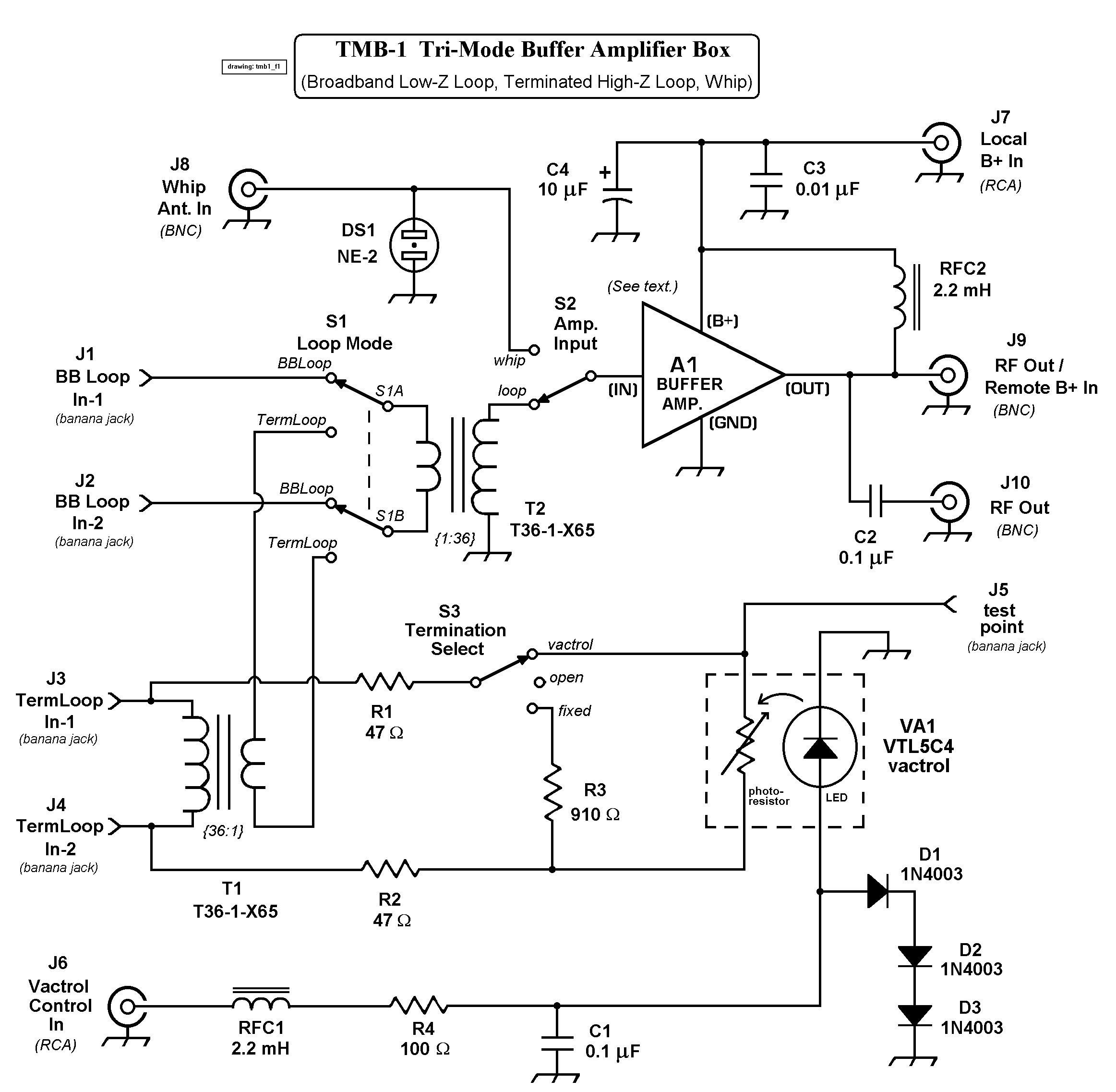
The TMB-1 is an RF amplifier unit and receiving accessory compatible with low-impedance broadband loops, high-impedance terminated loops (such as Pennant, Flag, or Kaz Delta), and whip (telescoping rod) antennas. This design is optimized for operation within the frequency...
The schematic shows R4 at the emitter of the transistor, as suggested by Amb and Majkel. It should be positioned between the operational amplifier and the transistor, which is also the correct configuration in the CanAmp. The amplifier observed...
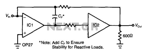
Adding a unity-gain buffer to an analog circuit can enhance its precision. For instance, the operational amplifier IC1 has a maximum offset voltage drift of 1.8 µV/°C and can drive a 600-ohm load. Under these conditions, IC1 would dissipate...