
Blocking material monitoring circuit

The blocking material monitoring circuit operates on the principle of detecting interruptions in an optical path using a phototransistor as the primary sensing element. Upon detection of a blockage, the circuit transitions through a series of states that control the operation of additional transistors and relays to signal an alarm condition. The use of a flip-flop configuration ensures that the state of the circuit is maintained even after the initial trigger condition (blockage) has been removed.
The choice of components is critical for optimal performance; transistors with a beta range of 50-80 are suitable for ensuring adequate current amplification. The constant current source formed by VT5 and the potentiometer RP is pivotal for the reliable charging of capacitor C2, which serves as a timing element in the circuit. The voltage across C2 must reach a specific threshold to activate the subsequent transistors VT6 and VT7, thus engaging the relay J1 for alarm signaling.
In practical applications, the circuit can be adjusted for sensitivity by modifying the value of the potentiometer RP or the resistance in series with the phototransistor. This allows for customization based on the specific requirements of the monitoring environment. Testing and debugging procedures are essential for ensuring the circuit functions as intended, particularly regarding the responsiveness of the relay when the optical path is obstructed. The integration of an automatic negotiation circuit with VT8 adds a layer of sophistication, allowing for dynamic response to varying conditions in the monitored environment. Overall, this circuit design provides an effective solution for monitoring the presence of blocking materials in various applications. Blocking material monitoring circuit is shown. When the optical path is blocked by the material, the phototransistor VT1 off, off transistor VT2, VT3, VT4 shoot coupled flip-fl op consisting of flip turned into VT3, VT4 off state, diode VD2 can not be turned on by the two groups are summarized di pole tube VT5 and potentiometer RP CzJ constant current source to charge the C2 voltage rises to a certain value composite pipes VT6, Vr7 turned on. J1 pull, external control circuit or alarm. If the voltage is not raised to make the C2 level VT6 conductive. Optical path through the old man, then flip into steady shot Xiang Tibetan VT3 deadline, VT4 conduction state, VD2 conduction, the capacitor Cz Chih-end clamped to a low potential, Jl not pull.
That can change the whole RP electric road blocking material to allow maximum time (ie, a short circuit is not blocking material alarm). VT8 light auto-negotiation for-profit composed of the alarm circuit. Component selection and commissioning follows. VT1 election 3DU5, VT2 ~ VT4, VT6 into 3DG6, betas between transistors 50-80. VI7 and VT8 selected 3DG12 or 3DK4. Lo values can be between 40-50. Jl and JZ selection JQX-4F type 1ZV relays or other sensitive relays. When debugging, the light shine on VT1 VT3 should deadline, Jl should be released, if not, you can change J9 VT2 large value (such as 100 -fold) transistors.
If the light path blocked Jl not pull a long time, it can be Ru, into a little resistance.
Related Circuits
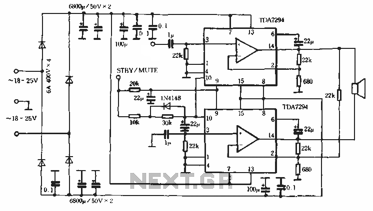
Europe's leading SGS-THOMSON STMicroelectronics recently introduced a new power integrated amplifier, the TDA7294, to the Chinese mainland market. This amplifier, characterized by a cold and hard tone, is particularly suited for Hi-Fi applications such as home theaters and active...
A two-tone generator that is alternately switched ON provides a high/low output similar to that of a traffic vehicle, such as a police car or ambulance. The CD4011 integrated circuit (IC1), which is a quad 2-input NAND gate, functions...
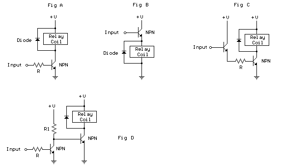
The schematic below illustrates four methods of controlling a relay with a digital logic signal. Figure A can be used in most cases where the relay coil requires 100 mA or less and the input current is 2 milliamps...
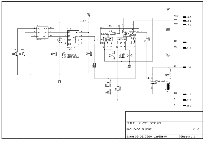
The following circuit illustrates a 2500W Phase Control Circuit Schematic. Features include a ground-tied trigger output that is disabled, and a low voltage input. The 2500W Phase Control Circuit is designed to regulate the power delivered to a load by...

The LED meter circuit is more compact and simpler than its analog equivalent, making it a common choice in audio equipment. This circuit utilizes the LM3915 integrated circuit (IC) and operates in a logarithmic mode. It comprises a single...
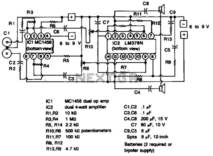
Even if the circuit is simple, it complies with all conditions regarding distortion and frequency response. The input resistance is 250K ohms, and it can drive loads ranging from 100 ohms to 2K ohms. The described circuit is a fundamental...