
Board making technique
The spacing between the signal pattern and the polygon is defined by a set value, which should not be smaller than the values specified by the Design Rule Check (DRC) or Net Class. The default spacing is set to 0 inches. The priority of a polygon is significant when multiple polygons overlap; smaller figures are assigned higher priority, with "1" indicating the top priority. After naming the polygon, clicking outside it allows for the entry of the grounding name. A dialog box appears upon clicking the OK button.
In outline mode, only the polygon's frame is visible around the PCB, while the polygon itself is not displayed. This mode is useful for modifying patterns. To revert to the original pattern, the Ripup button must be pressed, followed by switching to outline mode by clicking outside the board. The Ripup function returns the pattern to its original state, necessitating two steps for proper execution. Only the outline mode data is saved in the EAGLE file, while the actual display is processed through the CAM processor, initiated by the Ratsnest command. Outline mode is displayed upon restarting the project.
When changing the properties of a polygon or discontinuing its use, the polygon must be deleted. Although a polygon may appear to exist on the board, it is actually located at the periphery. The polygon's detailed drawing can be specified by width; however, excessive detail beyond the precision required for actual PCB production is unnecessary. The EAGLE manual suggests keeping the polygon width similar to that of other traces. Polygon patterns can be specified, with the default being solid; however, a hatch pattern can be used to reduce weight if desired.
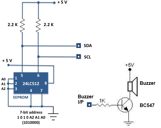
There are two methods for connecting the earth terminal to the ground pattern. The first involves integrating the terminal with the ground pattern without leaving a shape, while the second method connects the terminal shape while maintaining its outline. The latter is preferable for achieving clean soldering results. When a grounding polygon surrounds a signal pattern, there may be areas where a grounding polygon cannot be drawn. The decision to create a polygon in these areas must be made carefully, as polygons formed in such regions may not connect properly. In high-frequency circuits, these patterns can adversely affect circuit operation, making it essential to avoid creating polygons that fill these areas. The default value for isolation is set to 0, which indicates that the spacing between the signal pattern and the polygon should be determined by the larger value specified by DRC or Net Class.In case of making of a PCB, there is technique which makes a wide grounding pattern except the signal and power pattern. This technique is used for the circuit for the high frequency or when preventing an influence by the noise from outside, and so on.
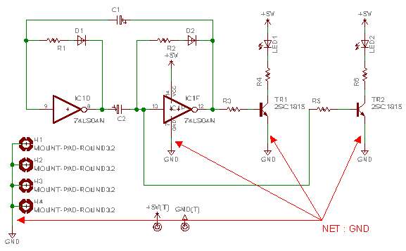
When making a printed board by the handwork, there is an effect which can rarely make the quantity of the copper to dissolve, too. When drawing a schematic, it makes the name of the grounding wire(NET) a GND. You can use a name except the GND. In my case, I am using a grounding symbol and because the symbol name is GND, the name of the wiring becomes GND automatically. This name is used for the name of the polygon. So, it`s better to confirm the name of the grounding wire by the Info command after drawing a schematic.
This is the interval specification between the signal pattern and the polygon. When this set value is smaller than the value specifying by DRC(Design Rule Check) or Net Class, either of DRC or Net Class a big value is used. The default is 0. The setting unit is an inch. This is the priority specifying of a polygon. It is effective when more than one polygon is piled up. When the figure is small, the priority is high. "1" is a top priority. After pushing the Name button, click the outside of the polygon and type the name of the grounding. A dialog on the right is shown when pushing the OK button. As for the outline mode, only the frame of the polygon is shown at the periphery of the board and the polygon isn`t drawn in the board.
This mode is convenient when changing a pattern and so on. Push the Ripup button at the time of the real mode. Next, it switches over to the outline mode when clicking the outside of the board. Because Ripup has the function to return a pattern to the origin, it is necessary to operate 2 steps. Only the data of the outline mode is recorded to the file of EAGLE. The displaying of a real mode is shown with the CAM processor from the data of the outlines. A CAM processor is started up by Ratsnest and real mode displaying is done. An outline mode is shown when restarting a project. When changing the property of the polygon or stopping the use of the polygon, the polygon must be deleted.
There seems to be a polygon in the board when drawing a polygon. However, the polygon in the board is not substance. The polygon is in the periphery of the board. Delete The detailed drawing of a polygon can be specified by Width. However, the polygon which was drawn in detail than the precision which makes an actual printed board doesn`t have a meaning. At the manual of EAGLE, it is referred to with "Typically you should keep the polygon width in the same range as your other wires".
The pattern of the polygon can be specified. Generally, it specifies Solid but in case of which wants to make weight light( ), and so on, it specifies Hatch. There are two kinds of ways of connecting between the earth terminal and the ground pattern. First, the method of making a terminal and a ground pattern incorporated and not leaving a shape. The 2nd, the method of connecting the shape of the terminal by leaving it. In case of the method of leaving the shape of the terminal, a terminal and a ground pattern are connected at four.
I think that it is better to leave the shape of the terminal to solder beautifully. When surrounding a signal pattern by the ground pattern polygon, the area where it isn`t possible to draw a ground pattern polygon sometimes exists. This is the specifying whether creates or doesn`t create a polygon to those areas. The polygon which was created in these areas is connected with nowhere. In case of the high frequency circuit, these patterns sometimes influence circuit operation. In the such case, it should not create the polygon to fill an area. The default value of Isolate is 0. In this case, the interval between the signal pattern and the polygon is drawn with the big value either of DRC or N
🔗 External reference
Related Circuits
A scoreboard is located in the center of the room, which will be controlled from backstage. The scoreboard features two individual 3-digit numbers. Whenever the score changes, a sound will be emitted. The simplest, most efficient, and cost-effective solution...
The laptop was damaged due to reversing the polarity of a universal power supply. A repair shop diagnosed a failed motherboard and quoted a replacement cost of €659, which was deemed excessive and ecologically unsound. The individual opted to...
All Things Pros discusses various topics related to patent prosecution. It provides strategies for addressing rejections under sections 102, 103, 101, and 112, often in the context of Board of Patent Appeals and Interferences (BPAI) decisions. The content also...
For beginners experiencing similar challenges, a general-purpose I/O board is recommended to minimize prototyping time and maximize space on the breadboard for projects. The construction of this board is straightforward. Basic I/O devices can be soldered onto a general-purpose...
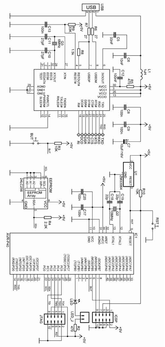
There are two ways to program AVR-P40-USB: with ICSP port and with JTAG port. To program via ICSP port you need serial port or parallel port AVR-ICSP programmer dongle (Olimex part # AVR-PG1B or AVR-PG2B). The serial port ICSP...
Build an interface board to connect scientific equipment, specifically a pair of photovoltaic tubes, to a personal computer for acquiring measurement results. The signal properties include two channels with a common ground, a one-second acquisition time, and a maximum...
Warning: include(partials/cookie-banner.php): Failed to open stream: Permission denied in /var/www/html/nextgr/view-circuit.php on line 713
Warning: include(): Failed opening 'partials/cookie-banner.php' for inclusion (include_path='.:/usr/share/php') in /var/www/html/nextgr/view-circuit.php on line 713