
Brake lights flasher circuits
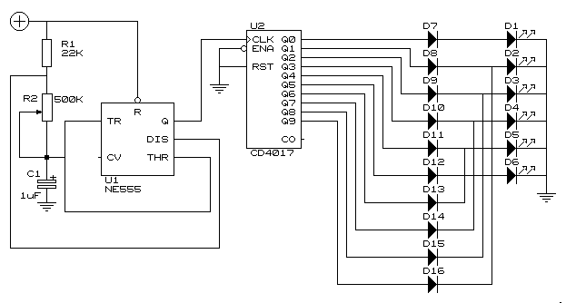
This brake light flashing circuit incorporates fundamental electronic components to achieve its functionality. The circuit begins with a 12V DC power supply, which is standard in automotive applications. The power enters the circuit and is filtered by capacitor C1 to eliminate any voltage spikes or noise, ensuring stable operation.
The heart of the circuit is the timer IC (IC2), which is configured to generate a pulse-width modulation (PWM) signal. This signal is output at pin 3 of IC2 and is responsible for driving the transistor (Q2). The transistor acts as a switch, allowing current to flow to the brake lights when activated. The frequency of the output pulse is primarily determined by the values of resistor R3 and capacitor C3, which set the oscillation rate.
As the brake is pressed, the output pulse is sent to the CD4024 (IC1), a binary counter IC. The pulses are counted until the circuit reaches eight counts, at which point the output at pin 2 of IC1 resets the counter, stopping the flashing sequence. The timing of the flashes is influenced by the configuration of capacitor C2 and resistor R1, which dictate the intervals between each flash.
In summary, this circuit design effectively allows for a visual indication of braking through flashing lights, enhancing vehicle safety. The ability to customize the timing components (R1, R3, C2, and C3) allows for flexibility in adjusting the flash rate and duration, making it adaptable to various user preferences or vehicle requirements. The choice of the transistor (Q2) is also flexible, permitting the use of different components while maintaining the circuit's functionality.This circuit will allow the brake light was flashing. The default behavior. When the power supply to the circuit, Or tap the brake it. The IC timer IC2 drive current to transistor Q2 and producing oscillator output, pulse signal output at pin 3 to input pin 1 of IC1-CD4024. Count pulse and stops counting after 8 pulses, with pin 2 of IC1 is reset. N ow, tap and hold the brake, the brake lights will flash the set, about 6 times per second. Which is determined by R3 and C3. The distance between each set, is defined by the C2 and R1. The Voltage input to the circuit, used 12 volt DC power from a car at all. The section capacitor C1 as a filter to smooth the flow. Transistor Q2 may be any number SM3180. 🔗 External reference
Related Circuits
This circuit is a simple -5V power supply using a 555 timer, designed for low-power analog applications involving FET operational amplifiers. The circuit converts +5V to -5V to create a dual power supply. It operates as a 555 astable...
These do-it-yourself FM transmitters are relatively simple to construct and provide a satisfying experience when music is played through the radio receiver. Comments and links to additional designs that are not included in the best list are welcome. FM transmitters...

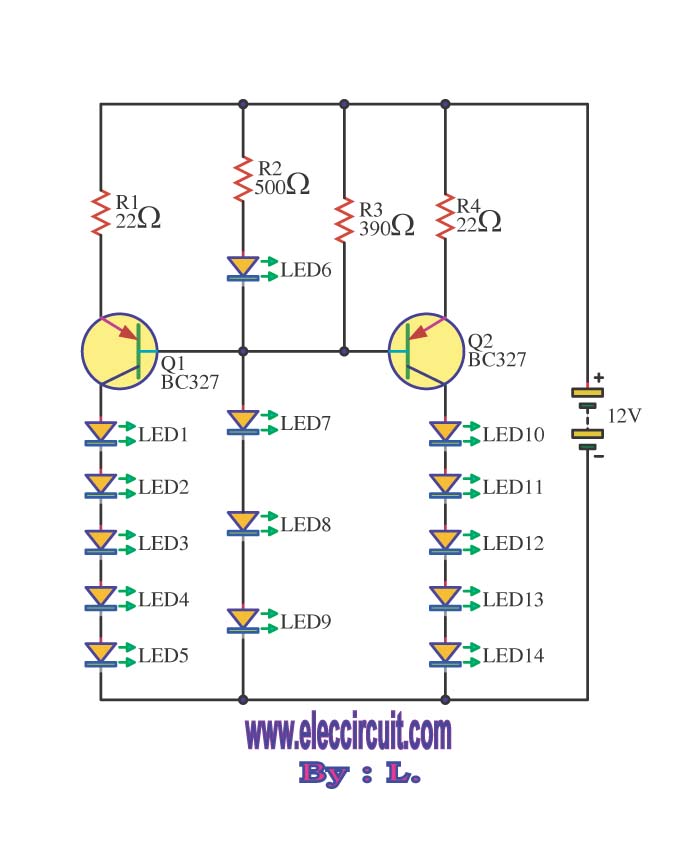
Circuits of this type are designed to drive LED arrays to enhance visibility and conspicuity when a vehicle is stopped or slowing down. This specific circuit emits a visual alert signal consisting of four short flashes followed by a...
The final article on bipolar junction transistors (BJT) presents a variety of circuits, some practical and others more experimental. These circuits are capable of amplifying signals, filtering high and low frequencies, generating white noise, and flashing lamps. They can...
This document provides a guide on understanding a simple computer system and its operation. It will examine the BASIC programming language and its statements, enabling communication with external circuitry. The document will also explore how to interface electronic circuits...
This circuit operates six LEDs in a "Knightrider scanner mode." The power consumption is primarily influenced by the type of LEDs utilized, especially when employing a 7555 (CMOS version of the 555 timer). Caution is advised when working with...