
Broadband using negative feedback amplifier circuit
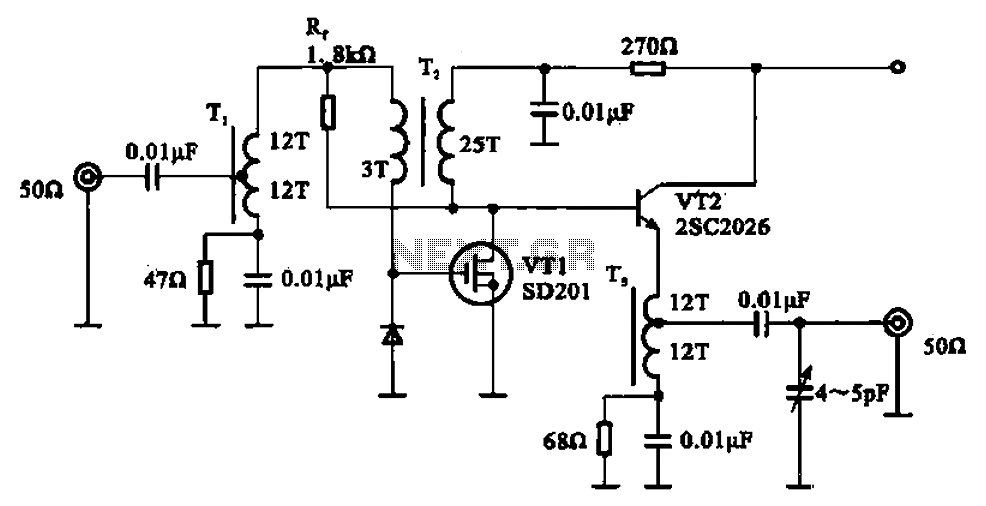
The broadband amplifier circuit described operates on the principles of negative feedback to enhance stability and bandwidth. The circuit's architecture is designed to ensure that the input signal is efficiently transferred through transformer coupling, which provides both impedance matching and isolation between stages. The use of field-effect transistors (FETs) allows for high input impedance and low output impedance, which is advantageous for minimizing signal loss and maximizing gain.
The transformer T2 plays a critical role in the circuit by facilitating the impedance transformation necessary for optimal signal processing. The primary winding receives the input signal, which is then coupled to the gate of the FET, allowing for effective amplification. The design ensures that the input impedance is adjustable between 50 ohms and 200 ohms, accommodating various source and load conditions.
Transistor VT1, connected to the secondary winding of transformer T2, operates under full load conditions, ensuring that the signal is amplified appropriately depending on the gain settings. The gain can be dynamically adjusted, providing flexibility for different applications. The secondary winding's gain is determined by the specific turns ratio, which is critical for achieving the desired amplification levels.
Transistor VT2, configured as an emitter amplifier, serves to further amplify the signal while maintaining a low output impedance. This configuration is essential for driving subsequent stages or loads without significant signal degradation. The output impedance can be fine-tuned through the coil tap at 5011, allowing for customization based on the specific requirements of the circuit or system in which the amplifier is implemented.
Overall, this broadband amplifier circuit exemplifies efficient design principles, utilizing negative feedback, transformer coupling, and FET technology to achieve high performance across a wide frequency range. Broadband using negative feedback amplifier circuit Shown as a negative feedback mode broadband amplifier circuit, the amplifier circuit are used transformer coupling, amplifyi ng section and sub-field effect transistor transistor combination. Circuit, the input signal is applied to the Ti coupling capacitor windings center tap, and then by the primary winding of the transformer T2 is applied to a field effect transistor gate on this way with an impedance conversion function, the input impedance increased to 50 n 200 n, the secondary winding of the transformer Tz group VT1 is very full load, depending on the gain of the amplifier T2 secondary winding (25/3 8,33). VT2 is emitter amplifier mode, the output impedance can be obtained through the coil tap 5011 selection.
Related Circuits

A power amp designed for use in low voltage, especially battery-operated, applications. For minimum parts count, C1 and C2 can be omitted. More: With pins 1 and 8 open circuit the gain in internally set to 20 dB. The described...
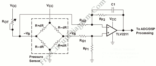
This is a pressure sensor signal conditioning circuit. It is a simple and inexpensive circuit due to its small geometry and the use of a straightforward pressure sensor. The pressure sensor signal conditioning circuit is designed to convert the raw...
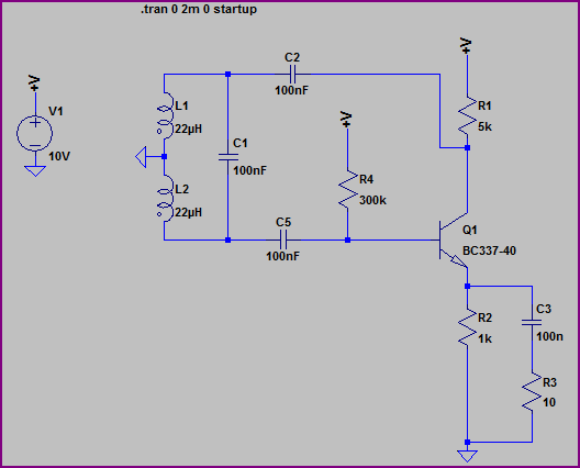
A Hartley Oscillator circuit can be constructed using a pair of series-connected coils. Two 22mH fixed inductors were utilized on a breadboard along with other necessary components. Testing the transistor amplifier independently indicated proper functionality; however, there is no...
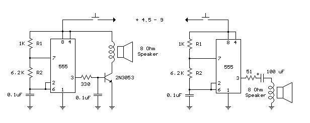
The following circuit is a basic 555 square wave oscillator. Features include a 1 kHz tone, simple circuitry, a current limit of 200 mA, reduced inductive voltage, and a supply voltage range of 4.5 to 9 volts. Components used...
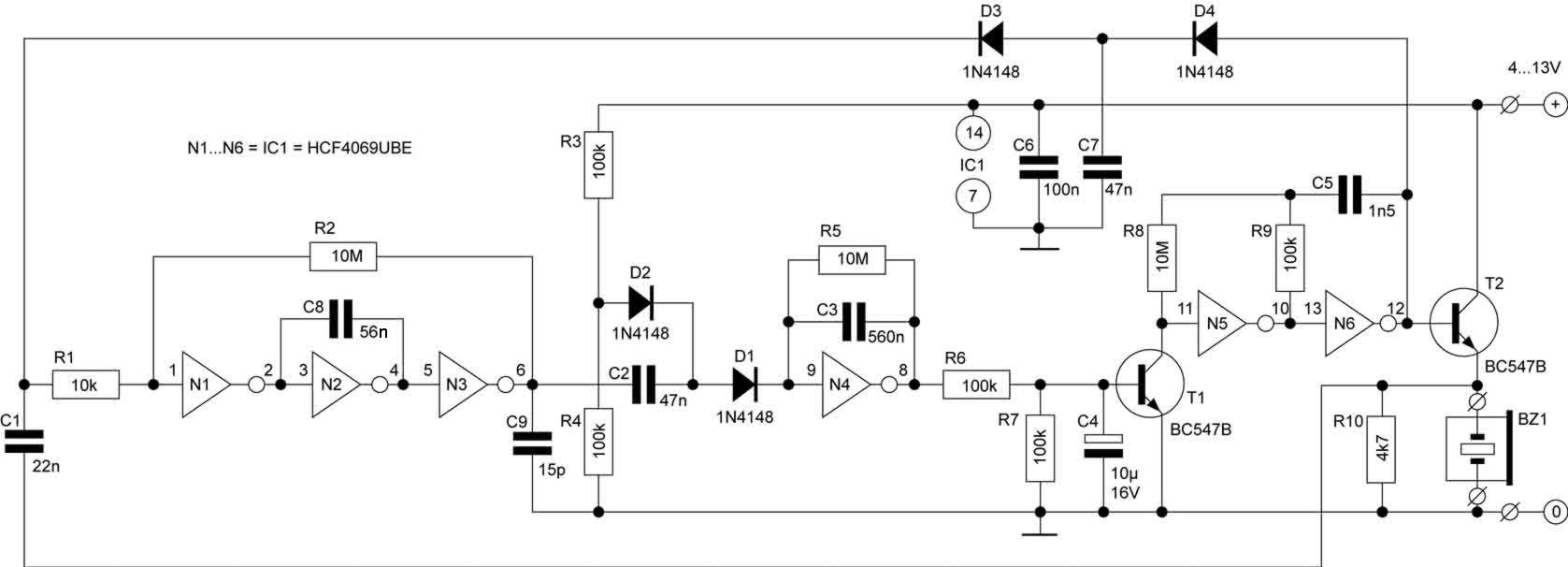
Picture a morning where you are anxiously waiting for the bus to work, only to realize that you cannot find your keys. If this scenario occurs often, this circuit is designed for you. A simple press of a button...
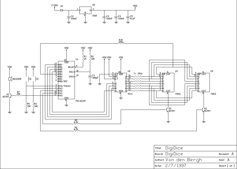
This is a digital dice circuit that uses the PIC16C84. The digital dice circuit utilizing the PIC16C84 microcontroller is designed to simulate the random rolling of a standard six-sided die. The circuit operates by generating a random number between 1...
Warning: include(partials/cookie-banner.php): Failed to open stream: Permission denied in /var/www/html/nextgr/view-circuit.php on line 713
Warning: include(): Failed opening 'partials/cookie-banner.php' for inclusion (include_path='.:/usr/share/php') in /var/www/html/nextgr/view-circuit.php on line 713