
Bus masters diagram
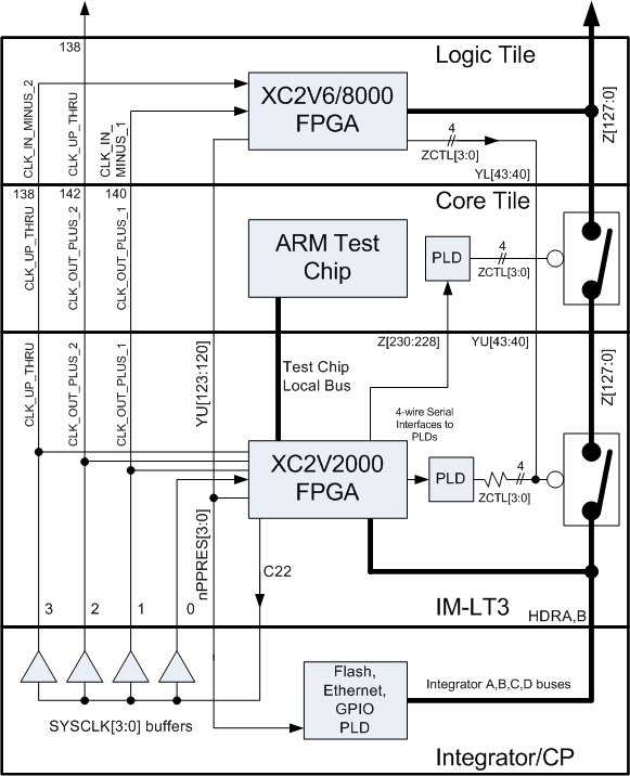
The proposed system enhancement involves modifying the existing AHB-Lite bus architecture to accommodate multiple bus masters. The AHB-Lite protocol is inherently designed for single master operation, which limits its flexibility in multi-master configurations. To implement additional bus masters, a bridging mechanism within the IM-LT3 FPGA is suggested. This entails the division of the Z[127:0] bus into two segments: an upper segment dedicated to custom bus masters and slaves, and a lower segment reserved for the existing AHB-Lite System bus controlled by the ARM CPU core.
The implementation of this architecture requires careful consideration of signal integrity and timing, as the introduction of additional masters may lead to increased contention for bus resources. The bridge in the IM-LT3 FPGA will facilitate communication between the two bus segments, ensuring that data can be routed effectively without conflicts. It is essential to design the bridge with appropriate arbitration logic to manage access to the bus and prevent data collisions.
Additionally, the custom bus masters will need to be compatible with the existing bus protocol to ensure seamless integration. This may involve implementing specific interfaces or protocols that allow these masters to communicate effectively with the AHB-Lite System bus.
In conclusion, while the integration of multiple bus masters within the AHB-Lite architecture poses challenges, the proposed solution of utilizing a bridge within the IM-LT3 FPGA offers a viable pathway to enhance system capabilities. This configuration not only expands the functionality of the Logic Tile but also maintains the integrity and performance of the existing AHB-Lite protocol.It is possible to add bus masters to the system, but a different bus architecture would be required, since the Integrator/CP uses the AHB-Lite bus protocol, which allows only one bus master (the ARM CPU core). One way to add bus masters in a Logic Tile would be to instantiate a bridge in the IM-LT3 FPGA, and splitting the Z[127:0] bus at the IM-LT3.
The custom masters (and slaves) could then exist on the upper segment of this bus, and the Integrator/CP's AHB-Lite System bus would continue to exist on the lower segment of the bus. 🔗 External reference
Related Circuits
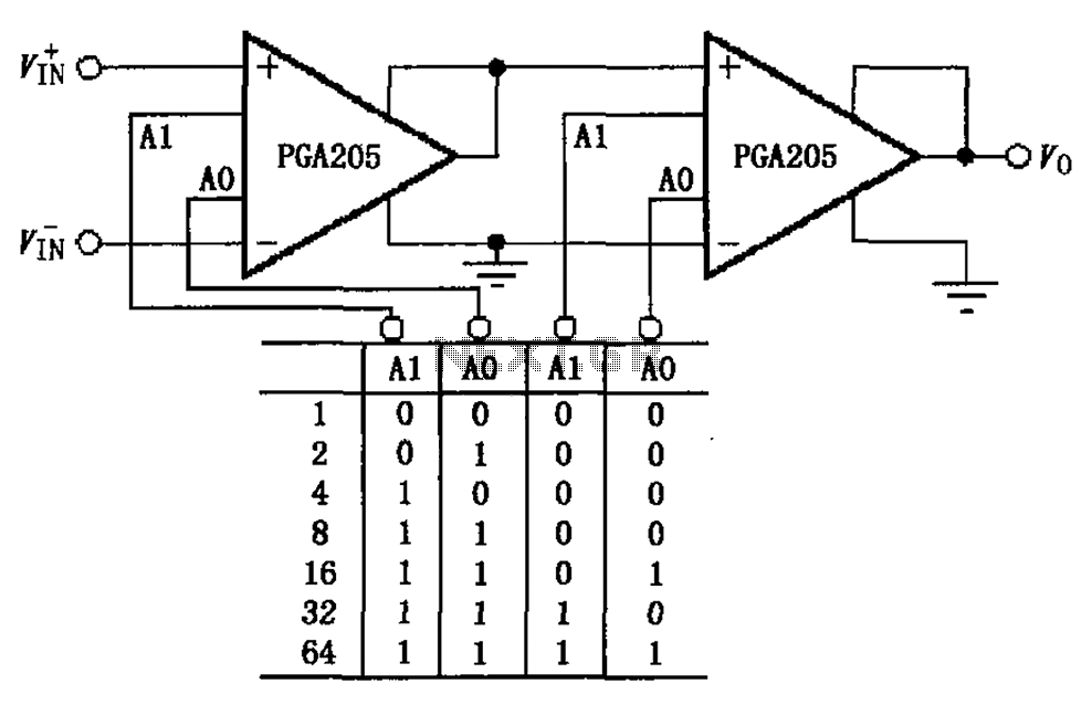
A binary gain step circuit is illustrated using the PGA205, which has a gain range of 1 to 64. The circuit employs two PGA205 devices in cascade, resulting in a total gain that is the product of the individual...
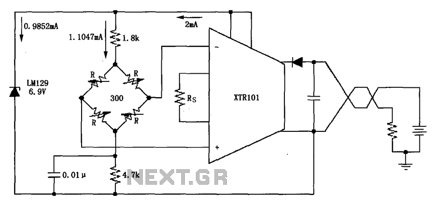
The circuit utilizes the LM129 voltage regulator to produce a 6.9V voltage reference, supplying a current of 1.0147mA from the 6.9V reference voltage to the bridge. The bridge may consist of varistor-type pressure sensors. The LM129 voltage regulator is a...
A 100W amplifier with a frequency range from DC to 500KHz features a photoelectric starting operational amplifier with high input impedance and high gain characteristics, enabling transformerless output power of 100W. The load current can reach up to 10A,...
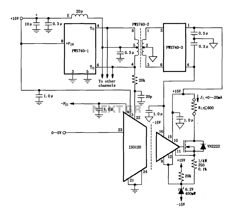
An eight-channel isolation circuit is constructed using the ISO120 and PWS740 components, designed for a 0 to 20 mA current loop. The figure illustrates only one channel, where the circuit converts a 0 to 5V input voltage into a...
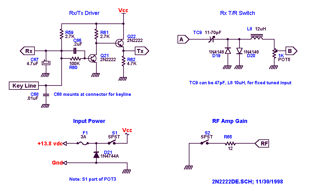
This section describes the components of the receiver, which includes the post-mixer amplifier, variable crystal filter, intermediate frequency (IF) amplifier, product detector, local oscillator, receiver muting, and audio amplifier. The transmit section features the local oscillator, transmit single balanced...
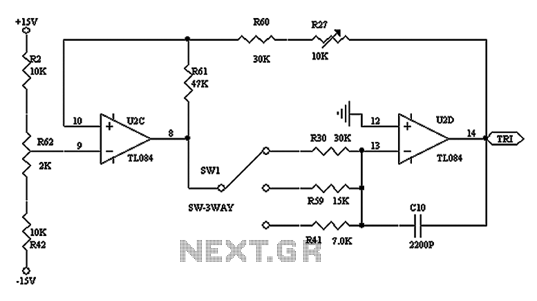
The triangular wave circuit consists of two operational amplifiers (OPs). R62 serves as the offset adjustment, while R27 is utilized for peak adjustment. A switch is included to select different resistances, allowing for the generation of triangular waves at...