
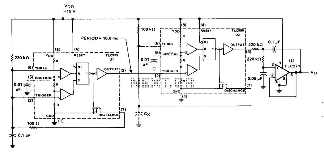
Capacitance to voltage meter
The diagram indicates that when the value of Cx is small, the duty cycle is relatively low. The output pulses are narrow, resulting in a lower average DC voltage level at the output of U3. As the capacitance of Cx increases, the duty cycle rises, causing the output pulses from U2 to widen and the average DC output level at U3 to increase. The graph plots capacitance values from 0.01 µF to 0.1 µF against the output voltage of U3, demonstrating excellent linearity and a direct one-to-one scale calibration of the meter. If linearity issues arise, the 100 kΩ resistor, R1, can be replaced with a potentiometer to allow for adjustment to the appropriate value for the meter being utilized.
The circuit features a free-running oscillator, implemented with timer U1, which generates a consistent frequency of 60 Hz. This frequency serves as the basis for generating trigger pulses for timer U2. Timer U2, configured in monostable mode, produces output pulses whose width is determined by the capacitance of Cx. The relationship between Cx and the duty cycle is critical, as it influences the average DC output voltage from U3.
Resistor R1, a fixed resistor, is essential for establishing the circuit's timing characteristics. Capacitor Cx, the component under measurement, directly affects the output characteristics of the circuit. The output of U2 is fed into U3, which acts both as a low-pass filter and a unity-gain follower. This configuration ensures that high-frequency components of the output pulses are attenuated, allowing for a smooth DC voltage output that reflects the average value of the pulse train.
The output from U3 is expected to exhibit linearity with respect to the capacitance values being measured. The described graph demonstrates this linear relationship, providing a clear calibration scale for the circuit. Should the output not align with the expected values, the inclusion of a potentiometer in place of R1 allows for fine-tuning of the circuit, ensuring accurate measurements across the specified capacitance range. This adaptability enhances the circuit's utility in various measurement applications.Timer Ul operates as a free-running oscillator at 60 Hz, providing trigger pulses to timer U2 which operates in the monostable mode. Resistor Rl is fixed and capacitor Cx is the capacitor being measured. While the output of U2 is 60 Hz, the duty cycle depends on the value of Cx. U3 is a combination low-pass filter and unity-gain follower whose dc voltage output is the time-averaged amplitude of the output pulses of U2, as shown in the timing diagram.
The diagram shows when the value of Cx is small the duty cycle is relatively low. The output pulses are narrow and produce a lower average dc voltage level at the output of U3. As the capacitance value of Cx increases, the duty cycle increases making the output pulses at U2 wider and the average dc level output at U3 increases. The graph illustrates capacitance values of 0.01 ?Â¥ to 0.1 ?Â¥ plotted against the output voltage of U3.
Notice the excellent linearity and direct one-to-one scale calibration of the meter. If this does not occur the 100 k ohm resistor, Rl, can be replaced with a potentiometer which can be adjusted to the proper value for the meter being used. 🔗 External reference
Related Circuits
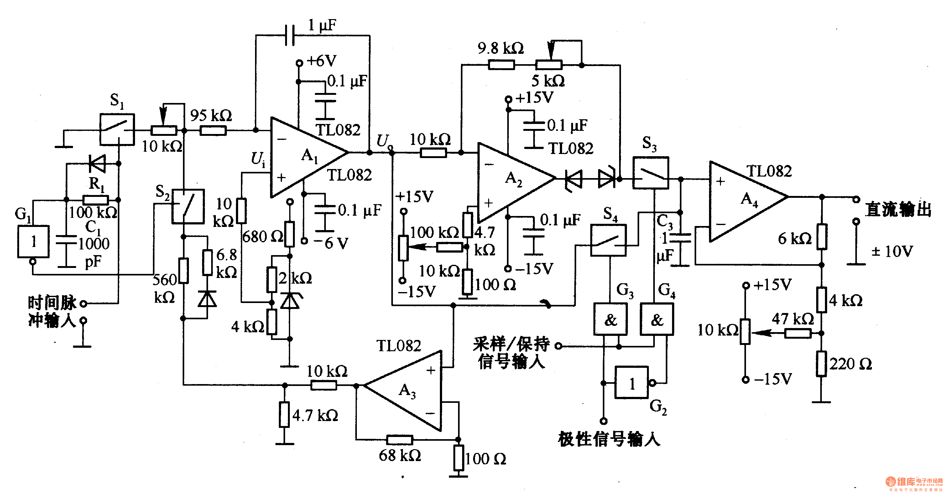
This circuit is designed for pulse width (time) to voltage conversion. According to the component parameters in the diagram, it can convert a pulse width of 0.1 seconds into an output voltage of 10V. When a conversion pulse is...
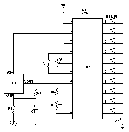
Any LED can be used for D1 - D10; however, blue LEDs require a higher voltage, which may result in them appearing dimmer compared to red, yellow, or green LEDs. If pin 9 of U2 is left disconnected, the...
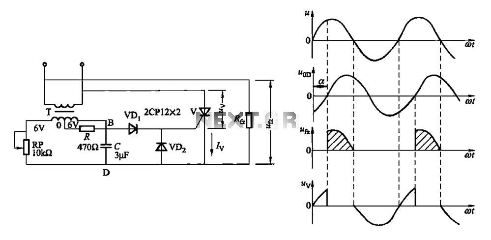
By adjusting the potentiometer RP, the output voltage of the phase shift bridge diagonal changes accordingly, which in turn alters the rectifier load power Rfz. Waveforms at respective points in FIG. 16-1 (b) illustrate this. Resistor R serves as...
The precision voltage-monitor chip features a temperature-compensated voltage reference. Resistor R1 divides the battery voltage to align with the built-in reference voltage of IC1 (15 volts). When the voltage at pin 3 drops below 15 volts, pin 4 provides...
This circuit is intended for precision centigrade temperature measurement, with a transmitter section converting to frequency the sensor's output voltage, which is proportional to the measured temperature. The output frequency bursts are conveyed into the mains supply cables. The...
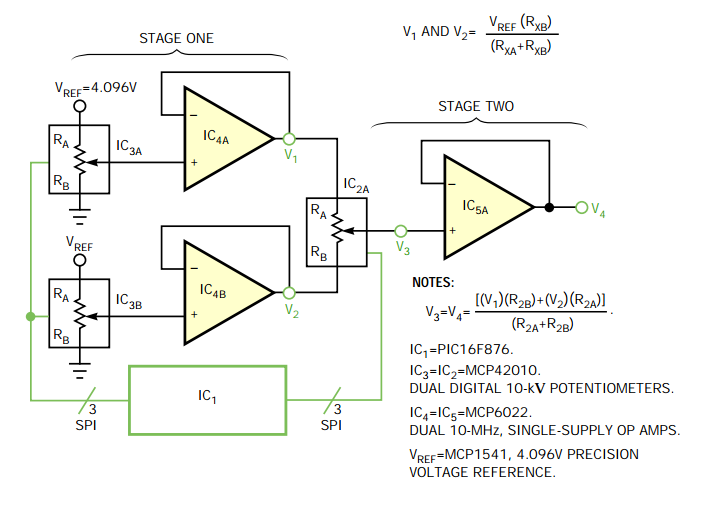
It may be easy to find a precision voltage reference for your application; however, a programmable precision reference is another matter. The circuit in Figure 1 yields a precision reference with an LSB of 62.5 µV. The circuit is...
Warning: include(partials/cookie-banner.php): Failed to open stream: Permission denied in /var/www/html/nextgr/view-circuit.php on line 713
Warning: include(): Failed opening 'partials/cookie-banner.php' for inclusion (include_path='.:/usr/share/php') in /var/www/html/nextgr/view-circuit.php on line 713