
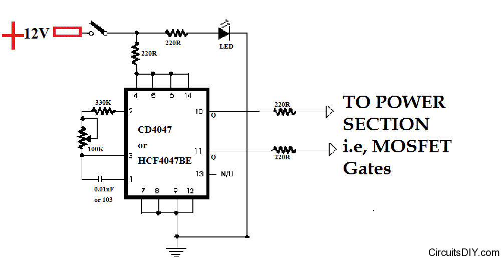
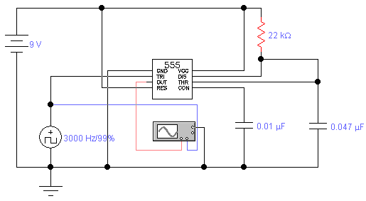
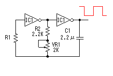
cd4047 based squarewave inverter oscillator
The circuit was originally designed with a 3055 NPN transistor, which has been replaced with an N-channel IRF540 MOSFET. A digital voltmeter (DVM) connected to the 220VAC output of the transformer shows only 20 volts, indicating a potential issue. It is noted that one MOSFET becomes excessively hot while the other remains cool. A request for assistance has been made regarding circuit functionality. Additionally, there is a need for guidance in designing a 50 Hz sine wave inverter, with a request for a complete circuit for a square wave inverter. It is suggested not to use zener diodes in series with Q1 and Q2; instead, a 4.7k resistor should be used in series for protection, with the zener diode placed after the resistor and grounded. Furthermore, a 5-watt rectifier diode should be added to the drain side of the MOSFET and grounded.
The feedback includes observations on circuit design choices, specifically regarding the use of diodes, where it is expressed that the two diodes may not serve a significant purpose. There is a discussion on the forward biasing of the diodes and their role in the circuit. The need for clarity in component symbols and simplification of the circuit by removing unnecessary parts is emphasized.
This square wave oscillator circuit employs the CD4047 IC, which is known for its versatility in generating square waves and can be configured for various frequencies. The circuit's efficiency is enhanced by utilizing MOSFETs, which have lower conduction losses compared to traditional bipolar junction transistors. The inclusion of protective diodes is critical, as they prevent back EMF generated by inductive loads from damaging the MOSFETs. The LED indicator serves as a visual cue for operational status, allowing for quick diagnostics.
The veroboard layout is practical for prototyping, enabling rapid testing and iteration before committing to a PCB design. This approach is particularly beneficial for beginners in electronics, as it simplifies the assembly process while still providing functional capabilities. The feedback regarding component choices and circuit behavior highlights the importance of understanding the role of each element in the circuit to optimize performance and reliability.
In summary, the circuit is designed to efficiently generate square wave signals suitable for driving MOSFET-based inverters, with considerations for component protection and diagnostics, making it a valuable resource for those venturing into inverter design.This simple and cheap(but powerful) squarewave oscillator can give oscillation to any mosfet based inverter/ups. The circuit consists of one central I. C CD4047. I used HCF4047BE from ST microelectronics. This is an improved version of circuit spread over the internet of inverter by I. C 4047. This circuit has more efficiency than that one. Here the MOSFET does not gets hot easily, and the Diodes IN4148 provides protection of the circuit in case of MOSFET leakage. A LED is added for easy diagnostics. Veroboard design of the circuit is given also, as we know, making PCBs is another dedicated work and we cannot make it in hurry.
Inspite of that, veroboard gives same functionality in lesser time(though size becomes a little big. ) Don`t post your email or phone number in the comment box. Only put email address in the email field. Comments are moderated so it may take time for them to appear on the site. Offensive comments will be deleted. If this is a request for custom circuit, then use the wish a circuit form. i tried to design this circuits but i have replaced 3055 npn transister to N-channel IRF540 Mosfet, i have attached DVM on 220vac output of tranformer, it display only 20 volts, this point to be also noted that 1 mosfet also too hot & 2nd one is normal cool, i have sent the circuit diagram on your gmail add, plz chech it, n tell me how does it work normally. first of all thank you for this circuit and now i need your help. i am new to this field and i am going to design 50 Hz sine wave inverter and for that i need basic ideas so plz will you upload or send me the complete circuit for squarewave inverter.
pls don, t use zener diode in Q1 and Q2 in series just attach 4. 7k resistor in Q1 and Q2 in series for protection just add zener diode after 4. 7K and ground the zener. in mosfet side @ drain side just add 5watt rectifier diode and ground the diode . hope you injoy my englesh thx Dear Arup, you have posted hundreds of circuits here and I have been following your site for a long time now. I am highly surprised to know that you decide on a device by looking at it`s package! So, if you see a small black package with three legs sticking out, you will call it a transistor Secondly, in my opinion, the two diodes in this circuit are not serving any purpose at all.
When the Q pins of the IC goes high, the diodes are forward biased and simply conduct the current into the mosfet gates. In fact, the post by warchen is the correct solution, but even he has forgotten to mention the zener diode voltage.
The zener diodes simply help in limiting the output voltage of the IC and produce a better and sharper square wave. And how have you decided that a 1N4148 can be considered as a 75 volt zener diode If you have any relevant information or literature on this, please let me know.
I don`t intend to be critical, but would be glad to help you in any way I can. Thanks 2. The question here is not of the reverse breakdown voltage of 1N4148, the question is what the hell is this diode doing here Even if we agree that it may act as a zener diode, but how is a 75V zener helping this circuit The operating voltage around this portion of the circuit is about 12V DC. Moreover, both the diodes are forward biased, so zener action does not arise. I don`t want to be too critical again, but let us be more practical and simplify the circuit by removing redundant components.
The least you can do is to change the zener diode symbol into a diode symbol at least. The article may be 2 years old, but your latest post was on 13 March, 2012 (about 17 days ago)but unfortunately you have not had the time to change the diode symbol in 2 years. 3. On a lighter note, I have a brotherly suggestion for your second point above . you shall have to increase the 10% reading to at least 60% reading, observing should not be more than be 25%, Guessing can remain at 10% and failing will automatically come down from a drastic 40% to a mere 5%.
If you are interested to know why I have reduced observation from 40% to 25%, you may contact me personally, my email address is with you. 🔗 External reference
Related Circuits
In this circuit, a CMOS inverter, such as the CD4069, is utilized to convert the open-drain Lx output into a signal that is appropriate for driving the gate of an external P-channel MOSFET. The MTP8P03 has a gate threshold...
This free-running multivibrator utilizes an external current sink to discharge the timing capacitor, C. As a result, the interval can easily be 1000 times the pulse duration, t1, which defines a positive output. The voltage across the capacitor, V,...
All the stages involved are designed to enable a frequency response of 20 to 100 kHz. Although such a high degree of frequency response is not necessary for this application, none of the stages have been eliminated as they...
The standard assumption is that the phase shift sections operate independently. According to the equation provided, the loop phase shift reaches -180 degrees when the phase shift of each section is 60 degrees. This condition is met when ω...
This circuit is a square wave oscillator that utilizes CMOS-type logic inverters. The term "logic inverter" is used to prevent confusion with a DC/AC inverter. The oscillator's output is connected to a drive circuit via the logic inverters. The...
The use of a quarter-wave parallel-wire line as a tuning unit has been discussed in the chapter on Short-Lines, where it was pointed out that these circuits have comparatively high Q even at higher frequencies. Their significant length (approximately...