
digital modified sine wave inverter
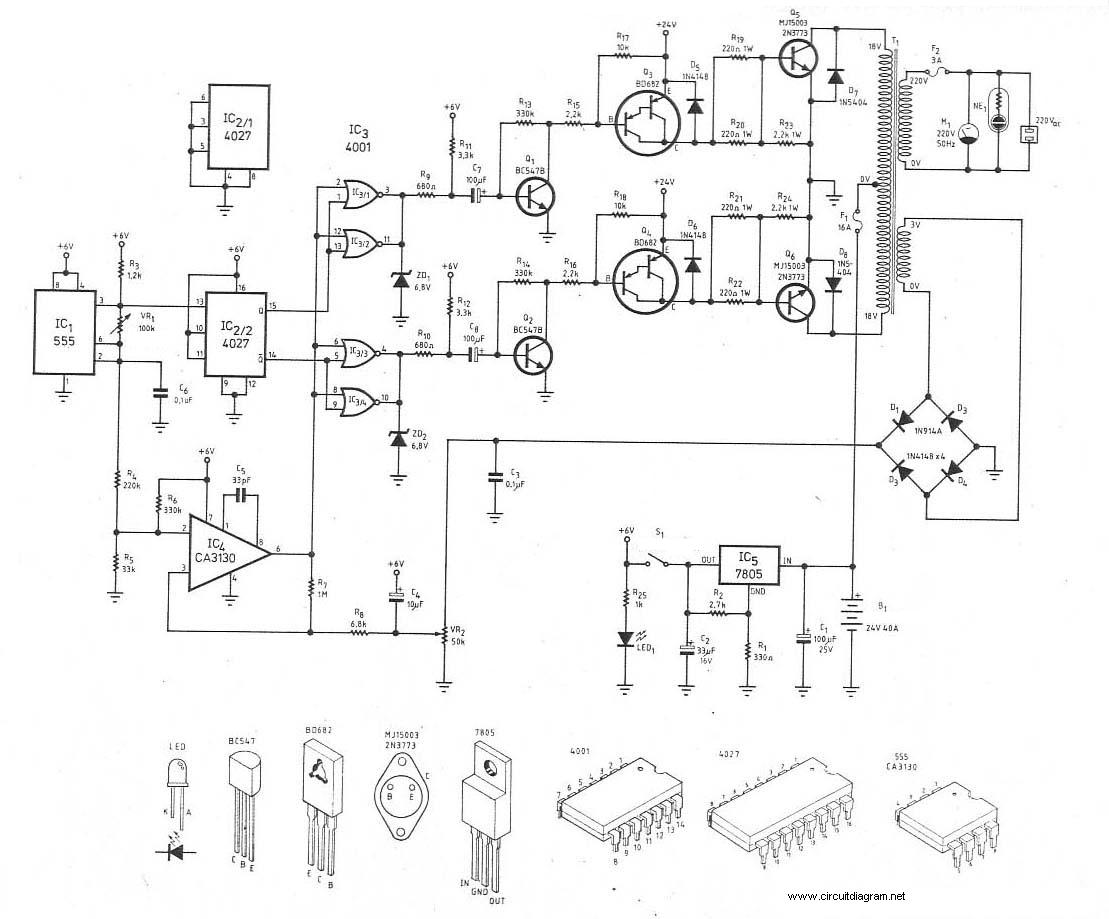
The circuit described is a multi-stage amplifier designed to operate within a frequency range of 20 to 100 kHz. The initial stage utilizes BC556 transistors configured as a differential amplifier, which provides the necessary gain while maintaining linearity. This stage is crucial for minimizing noise and improving signal integrity, especially in applications requiring precision.
Following the differential amplifier, the circuit transitions to a driver stage composed of BD140 and BD139 transistors. This stage is responsible for driving the output stage effectively, ensuring that the signal is strong enough to control the subsequent MOSFETs. The balanced configuration of the driver stage helps to maintain signal fidelity and reduce distortion, which is particularly important in high-frequency applications.
The output stage employs high-power MOSFETs, which are selected for their ability to handle significant current and voltage levels while maintaining efficiency. This stage is pivotal for delivering the final amplified signal to the load, which in this case is a transformer used in the inverter circuit. The use of MOSFETs allows for rapid switching, making them ideal for PWM applications, where precise control over the output waveform is required.
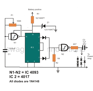
To optimize the performance of the inverter circuit, a well-dimensioned PWM input is necessary. This input modulates the output signal, allowing for the generation of a digital sine wave, which is essential for many inverter applications. Additionally, the circuit includes a diode at the output that can be selected to reduce the amplitude of the output signal. This selection is crucial for adjusting the RMS level of the transformer output, ensuring compatibility with the load.
The output waveforms generated by the circuit can vary based on the selection of diodes at the oscillator stage. Each configuration will produce different RMS values, which must be carefully evaluated to ensure that the power inverter circuit operates efficiently and reliably. Proper selection of these components and configurations is vital for achieving the desired performance characteristics in the final application.All the stages involved are actually for enabling a frequency response of 20 to 100kHz, though here we wont need such high degree of frequency response, I didnt eliminate any of the stages as it wouldnt do any harm to the circuit. The first stage consisting of the BC556 transistors is the differential amplifier stage, next comes the well balanced
driver stage consisting of the BD140/BD139 transistors and finally its the output stage which is made up of the powerful mosfets. This completes the power amp stage, however this stage requires a well dimensioned input, rather a PWM input which would ultimately help to create the proposed digital sine wave inverter circuit design.
One of the diodes at the output may be selected for reducing the amplitude of the output signal which would ultimately help in adjusting the RMS level of the transformer output. The figure below shows various waveforms outputs as per the selection of the number of diodes at the output of the oscillator stage, the waveforms may have different relevant RMS values, which must be carefully selected for feding the power inverter circuit.
🔗 External reference
Related Circuits
This is the schematic diagram of a 300W power inverter circuit. The inverter utilizes the MJ15003 power transistor for final amplification. If the MJ15003 transistor is difficult to source, it can be replaced with a 2N3773. The inverter is...
The 50W inverter circuit is built using the power MOSFET FQB45N03 and the IC TL494. This inverter converts a 12-14V DC input from a car battery into a 220V AC output with a 50Hz sine wave frequency. The main...
Assistance is required for a final year project involving the design of a grid-connected inverter. The focus is on developing a full bridge inverter circuit. The grid-connected inverter is a crucial component in renewable energy systems, particularly in solar photovoltaic...
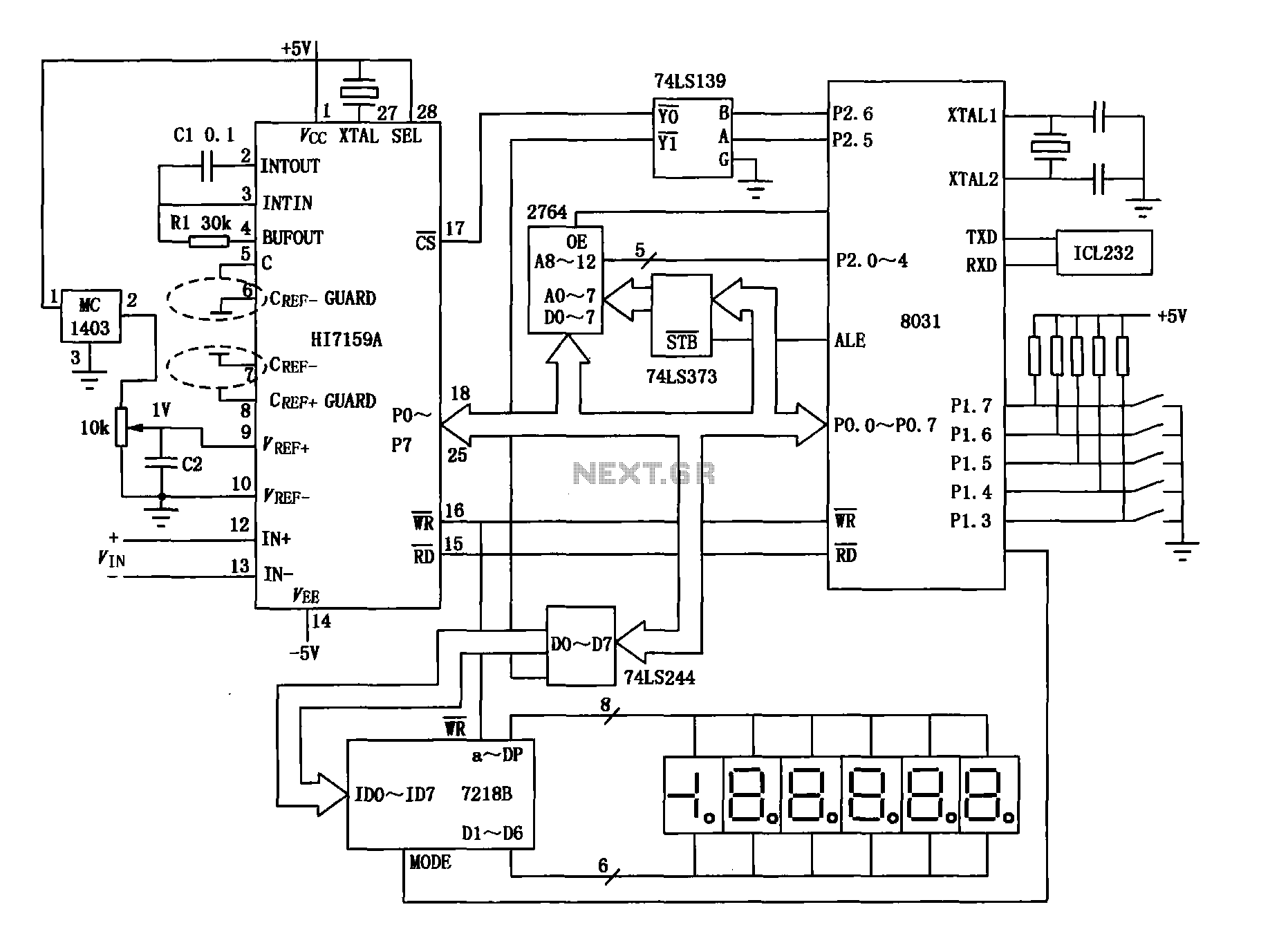
An intelligent digital voltmeter circuit utilizing the HI7159A, 8031 microcontroller, and various other components as illustrated in the figure. The internal circuit incorporates a successive cumulative integrator, digital zero function, low noise BIMOS technology, and other advanced features. In...
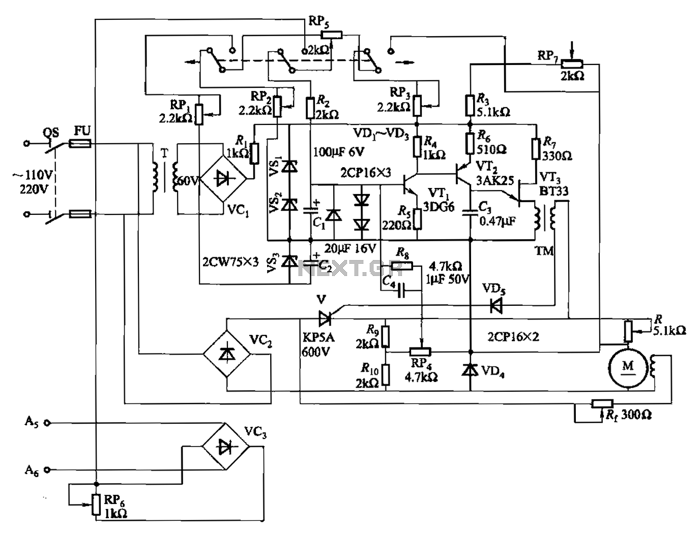
A 100W full-wave single-junction transistor trigger control circuit designed for constant or variable speed control of a wire feed motor. The input control signal consists of a voltage adjusted by the master potentiometer (RPs) and a feedback voltage from...
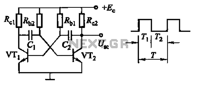
Common non-sinusoidal oscillator circuit, waveform and frequency formula - square wave oscillator - self-excited multivibrator The common non-sinusoidal oscillator circuit, specifically the square wave oscillator, is a fundamental electronic circuit utilized to generate square wave signals. It operates based on...
Warning: include(partials/cookie-banner.php): Failed to open stream: Permission denied in /var/www/html/nextgr/view-circuit.php on line 713
Warning: include(): Failed opening 'partials/cookie-banner.php' for inclusion (include_path='.:/usr/share/php') in /var/www/html/nextgr/view-circuit.php on line 713