
Checking out the Pierce oscillator
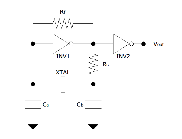
The Pierce oscillator is characterized by its simplicity and effectiveness in generating stable oscillations, particularly when utilizing crystal oscillators. The core of the circuit consists of a single inverter, which is configured to operate in its linear region, allowing it to amplify the oscillating signal generated by the crystal. The feedback resistor (Rf) plays a crucial role in maintaining the inverter's linear operation, ensuring that the circuit can sustain oscillations without entering a digital state.
In terms of component selection, the inverter should ideally be a buffered type to reduce power consumption and increase gain. The output signal is taken from the inverter, which can be further processed using additional components, such as Schmitt triggers, to refine the signal quality. The choice of resistors and capacitors is critical; Rs must be carefully calculated to balance crystal drive and noise immunity. The interaction between Rs and the capacitors (Ca and Cb) is essential for achieving the desired phase shift necessary for stable oscillation.
The capacitors not only influence the gain but also determine the frequency stability of the oscillator. By adjusting the values of Ca and Cb, one can fine-tune the oscillator's performance to meet specific application requirements. The load capacitance specified by the crystal manufacturer must be adhered to, ensuring optimal performance and reliability.
Overall, the design of a Pierce oscillator requires a careful balance of theoretical knowledge and practical experimentation. The iterative process of testing and refining component values is integral to achieving a successful oscillator circuit that meets the desired frequency and stability criteria.The Pierce oscillator is a very simple circuit and as with the ring oscillator also uses inverters (actually just one inverter will do). The principle of operation, however, is very different. While the ring oscillator exploits the incremental propagation delay through the series of inverters, the Pierce oscillator puts the inverter/gate into the
linear region of operation and employs it as an analog amplifier. To find out the details of the gate-based Pierce oscillator I recommend reading the references listed below. What follows is just a summary of the tips and formulas culled from the said references, pointers and tidbits which I found useful in getting a crystal-based oscillator up and running.
I also did a number of breadboarded experiments and the results are shown below. INV is of course the inverter (buffered or unbuffered). Oscillator signal is taken from the inverter output (Vout). To improve (decrease) its rise/fall time, another inverter or, better yet, a (fast!) Schmitt trigger can be used to spruce up the signal. The signal at the inverter input is a sinusoid and can also be used (some Microchip MCU datasheets show the clock signal being derived from the input of the inverter while other Microchip datasheets show it being taken from the inverter output).
Rf is a feedback resistor that puts the gate in linear (as opposed to digital) mode operation. The following table provides a rule of thumb value for Rf given crystal frequency: Among other things, Rs limits the amount of crystal drive-increasing Rs decreases drive. A ballpark figure or first cut value for Rs can be derived by computing for and equating Rs to the reactance of Cb: Rs is typically 40 K ohms or less, but is almost never more than 100 K ohms.
If the value for Rs is too high, then the high impedance input side of the amplifier may be more susceptible to noise, very much the same way a pull-up resistor on an input pin is normally kept below about 50 K ohms to prevent noise from having enough strength to override the input. Freescale (Motorola) meanwhile claims that for low frequencies such as 32. 768kHz watch crystals, Rs can go as high as 330Kohms. Because of a permissible maximum drive of just 1 µW, a minimum Rs value for tuning fork crystals such as the 32.
768kHz crystal is 10kohm. Ca and Cb along with Rs and XTAL provide a 180 degree phase shift (INV provides the other 180 degrees for a total of 360). Moreover, the Rs and Cb network partly "acts as a low pass filter that discourages the crystal from running at a third or fifth harmonic, or other higher frequency" (Lancaster and Berlin).
Increasing Ca and Cb decreases the gain. Ca and Cb are usually equal but Cb can be made larger than Ca. The voltage at the input of INV is (partly) determined by Cb / Ca, so that increasing Cb relative to Ca increases the voltage at INV input. As a rule the values of Ca and Cb should satisfy the following condition: where Cload is the load capacitance of the crystal as per manufacturer`s specifications.
Typical load capacitances are 12 pF, 15 pF, 18 pF, 20 pF, 22 pF and 32 pF. Finally, an advice worth keeping in mind: "Oscillator design is an imperfect art at best. Combinations of theoretical and experimental design techniques should be used. " And so we move on to the experimental side of things. I performed a few tests on a breadboard using 4. 000 MHz and 32. 768 kHz crystals. The values for the resistors and caps are the ones I arrived at after some trial and error. The values below seem to work better. Yes, that`s a very subjective assessment and shall leave it at that. II. National Semiconductor MM74HC02N quad 2-input NOR gate. Unfortunately, I don`t currently have any CMOS HC or AC series inverters. According to the datasheet each NOR gate is buffered as follows: Using a buffered gate in a Pierce oscillator consumes less power and has a gain in the order of thousands compared to an unbuffered ga 🔗 External reference
Related Circuits
The output of a video amplifier is differentiated before being fed to a Schottky comparator. The propagation delay is typically reduced to 10 ns. The output pulse width is determined by the value of C, 10 pF, resulting in...
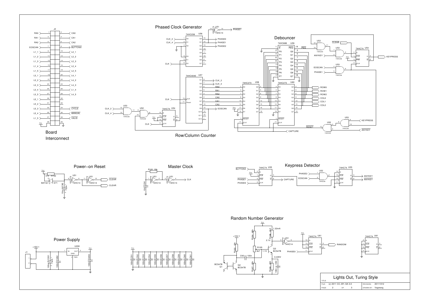
The design is based on the previous analysis of calculating the game in a circular shift register. While designing, it was realized that small extensions to the design would enable additional gameplay features, such as replay and manual input....

An electronic circuit consists of individual electronic components such as resistors, transistors, capacitors, inductors, and diodes, which are interconnected by conductive wires or traces that allow electric current to flow. The sine wave or sinusoid is a mathematical function...
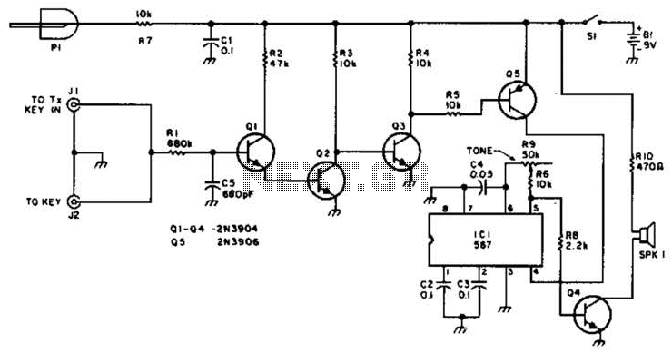
For use with low-power transmitters that require a positive keying voltage. The transistors Q1, Q2, and Q3 are configured as a switching amplifier. When the key is pressed, the collector of Q3 is pulled to ground, which activates Q5...
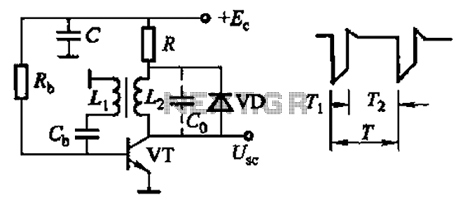
Common non-sinusoidal oscillator circuit, waveform and frequency formula - sawtooth oscillator - use blocking oscillator The sawtooth oscillator is a type of non-sinusoidal oscillator that generates a waveform characterized by a linear rise in voltage followed by a rapid drop....
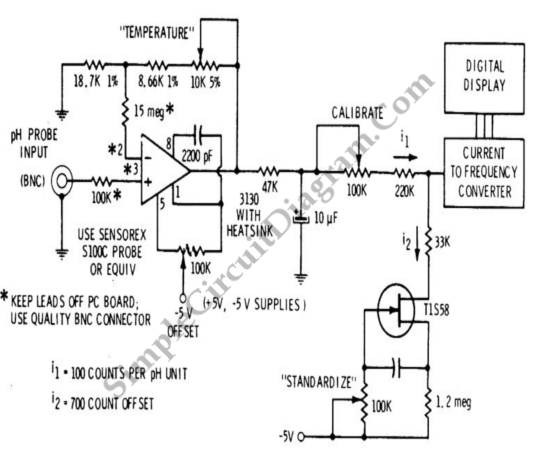
A signal conditioner for a pH meter probe requires high input impedance. The signal conditioning of the pH meter probe is achieved by incorporating a buffer. The design of a signal conditioner for a pH meter probe is critical for...