
Circuit operation explanation of astable multivibrator
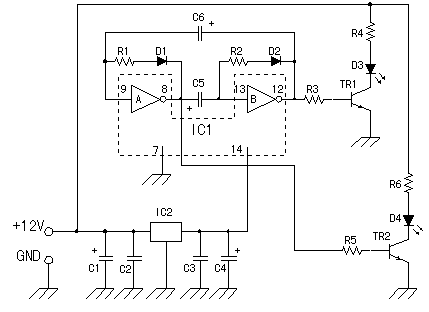
The circuit employs a feedback mechanism utilizing two inverters, specifically the 74HC04, to create a self-oscillating configuration. In this arrangement, inverter A and inverter B are interconnected, allowing for the dynamic control of their states based on the charge and discharge cycles of capacitors C5 and C6. The feedback loop formed by resistor R2 and diode D2 ensures that the output of inverter B influences its input, thereby enabling oscillation.
The timing of the oscillation is primarily determined by the capacitance values of C5 and C6 and the resistance value of R2. The charge time and discharge time of the capacitors dictate the frequency of oscillation. The threshold voltage (VT) of the inverters is crucial as it sets the levels at which the inverters switch states. If the input voltage falls below VT, the inverter output will transition low, while exceeding VT will result in a high output.
In practical applications, the circuit is sensitive to component tolerances and variations in supply voltage, which can affect the oscillation frequency and stability. The behavior observed with the 74HC04, where both LEDs lit simultaneously, suggests that the circuit may not have achieved a stable oscillating state, possibly due to improper biasing or component values not being optimized for the desired frequency.
To analyze the circuit further, the relationship between voltage, current, and the time constants associated with the RC circuit can be expressed mathematically. The electric current (I) through the resistor can be calculated using Ohm's law, while the voltage across the capacitor can be described by the formula \( V(t) = V_0(1 - e^{-t/RC}) \), where \( V_0 \) is the initial voltage, \( R \) is the resistance, \( C \) is the capacitance, and \( t \) is time. This mathematical framework aids in understanding the transient response of the circuit and optimizing component selection for desired operational characteristics.It doesn`t break if being little even if it crosses the value of the input/output electric current characteristic. It breaks when short-circuiting and doing the extreme thing in the output. It is explained by the following circuit operation but because the input electric current must flow little at the circuit this time, 74HC04 can not be used.
First, I assume that the input (the 9th pin) of the inverter A is the low level. At this time, the output (the 8th pin) of the inverter A becomes high level. At first, the condition of the inverter B is unsettled but because the output of the inverter B is not totally in the high level condition, above-mentioned electric current flows. When the electric charge begins to store up in C5, C5 can be seen like the short circuit condition. Because it is, the input of the inverter B becomes the high level condition. The output of the inverter B becomes the low level and above-mentioned electric current route is totally formed by this operation.
When the electric charge is stored up in C5, the electric current decreases. Input voltage of the inverter B, too, goes down with it and approaches the threshold voltage of the inverter B. Because the output of the inverter B is the low level (being 0V almost), the electric current alwayses fall through more through R2, D2 and the input voltage of the inverter B becomes the threshold voltage (VT).
The output of the inverter B is conveyed to the input of the inverter B through R2 when there is not D2. Then, it repeats the operation that the input of the inverter B becomes high level again and that the output becomes the low level and the inverter B has worked in the oscillation.
The high level output of the inverter B makes the input of the inverter A the high level condition through C6. At this time, the electric current flows with the inverter B output When the input of the inverter A becomes the high level condition, the output of the inverter A becomes the low level.
The electric charge that the side of the output of the inverter A is positive already is stored up in C5. Because the output of the inverter A becomes the low level (0V) in the condition, the voltage on the side of the input of the inverter B starts from the negative potential.
When the electric charge is stored up in C6, the electric current decreases and input voltage of the inverter A goes down. When the input voltage of the inverter A becomes the threshold voltage, the output of the inverter A becomes high level.
When turning on, the condition of the inverter isn`t decided. Each inverter characteristic isn`t the same. The output of either the inverter becomes high level earlier and it fixes the condition. When there is an ideal inverter circuit, it is possible to think of repeat`s not being worked, too. However, actually, there is not such one and it works repeatedly. When it isn`t possible to do this discharge, at the next period, because the electric charge starts from the stored condition, the input voltage of the invertor becomes the threshold voltage immediately. That is, the period of the repeat becomes short or the repeat isn`t done. The period doesn`t sometimes become long without discharge`s being sufficiently done even if it makes the value of the capacitor big to make the repeat period long, too.
Indeed, I attempted to work the circuit using 74HC04. At first, seemingly, it did the normal operation, but both LEDs lit up at the same time and didn`t do the normal operation in case of being for a while. The electric current change when the voltage (V) is applied to the circuit which the capacitor (C) and the resistor (R) were connected with in series can be demanded by the following formula.
🔗 External reference
Related Circuits

This LED VU Meter (volume unit) is designed to monitor and display power levels present at the speaker terminals of a stereo audio power amplifier. The levels are represented in ten discrete steps using ten LEDs for each channel,...
Humidity detector circuit electronic project using common electronic parts The humidity detector circuit is a project designed to measure and indicate the level of humidity in the environment. This circuit utilizes commonly available electronic components, making it accessible for hobbyists...
The transistor is configured as an audio oscillator, utilizing an audio transformer in the collector. The secondary winding is connected to a linear potentiometer. The ratio between the two sections of the potentiometer from the slider is proportional to...
Samsung C3330 Circuit Diagram Download Manual PDF Download. The Samsung C3330 circuit diagram serves as a comprehensive reference for understanding the electronic architecture of the device. This schematic provides detailed insights into the interconnections between various components, including the microcontroller,...
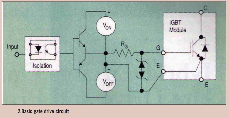
High power IGBT modules utilize hybrid integrated circuit (IC) gate drives that incorporate protection circuits, which implement desaturation detection or real-time control. High power Insulated Gate Bipolar Transistor (IGBT) modules are essential components in various high-efficiency power conversion applications, such...

The count switching circuit consists of an electronic switch and a pulse delay circuit for control. The count switching circuit is designed to manage the switching of signals in a controlled manner. The electronic switch serves as the primary component...