
3 Input Mic Mixer Circuit
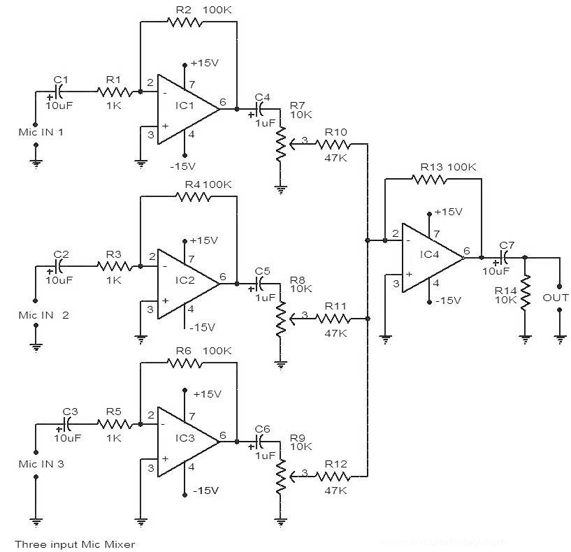
The circuit utilizes four operational amplifiers from the 741 IC series, which are well-known for their versatility in audio applications. The primary function of this mixer circuit is to combine audio signals from three different microphones into a single output, allowing for a unified audio feed.
IC1, IC2, and IC3 are configured as non-inverting amplifiers, each receiving input from a separate microphone. The gain of each amplifier can be adjusted through the use of external resistors, ensuring that the output levels from each microphone are balanced. This is particularly important in applications where microphones may have different output sensitivities.
The fourth 741 IC (IC4) is employed as a summing amplifier, where it takes the outputs from the three non-inverting amplifiers and combines them into a single output signal. This configuration allows for effective mixing of the audio signals, maintaining the integrity of each input while enhancing overall sound quality.
Power supply connections for the 741 ICs typically involve dual power supplies, often +15V and -15V, to accommodate the operational range of the amplifiers. Bypass capacitors are recommended at the power supply pins of each IC to minimize noise and ensure stable operation.
The output from IC4 can be further processed or sent directly to a speaker or recording device. Additional components such as capacitors and resistors may be included in the circuit to filter out unwanted frequencies and improve the overall audio quality.
This 741 IC-based microphone mixer circuit is suitable for various applications, including live sound reinforcement, studio recording, and broadcast environments, providing a reliable solution for mixing multiple audio sources.Here is the circuit diagram of a 741 IC based 3 input mic mixer ckt. Altogether four 741 IC`s are used out of which IC1, IC2, and IC3. 🔗 External reference
Related Circuits
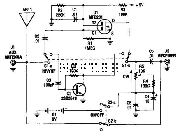
The AA-7 active antenna consists of two active components: Q1 (an MFE201 N-channel dual-gate FET) and Q2 (a 2SC2570 VHF silicon transistor), which form the foundation for two independent, switchable RF preamplifiers. The AA-7 active antenna is designed to enhance...

A 555 IC is configured to function as a Schmitt trigger. Inputs above and below the threshold level will turn the circuit on and off, producing a square wave output. The 555 timer integrated circuit (IC) is a versatile device...

This picture and schematic were intended for posting on my Watson's blog, but it did not get published. The circuit schematic in question likely includes various electronic components arranged to perform a specific function. Typically, such schematics are used to...
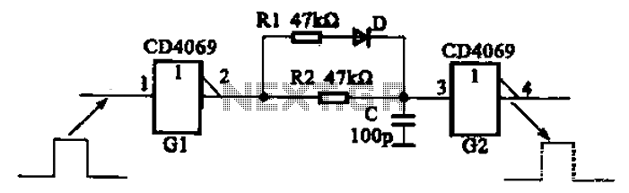
The inverter circuit using CD4069 is configured with a delay and width adjustment. When the output of the inverter (G1) is high, the capacitor (C) charges through resistor (R1) and diode (D). The voltage across capacitor C quickly reaches...
When the switch SI is pressed, the silicon-controlled rectifier (SCR) is activated, connecting LED1 and resistor R1 across the telephone line. This action causes the line voltage to drop to approximately 20 volts, which maintains the connection to the...
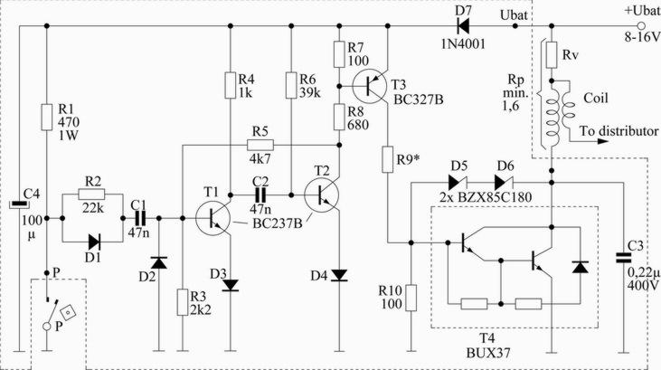
This scheme is designed for a four-cylinder engine. It aims to reduce fuel consumption, increase speed slightly, and minimize the need for frequent access to the distributor cap for contact button replacement, thereby saving costs. Transistors T1 and T2...