
Buffer Circuit Schematic Diagram

The circuit utilizes a Darlington pair configuration for its buffer stage, which consists of two bipolar junction transistors (BJTs) connected in such a way that the current amplified by the first transistor is fed into the second transistor. This arrangement allows for a high current gain, making it suitable for applications requiring significant output current while maintaining low output impedance. The circuit's design ensures that the input signal is effectively buffered, preventing loading effects that could degrade signal integrity.
The resistor connected to the base of the first transistor plays a crucial role in setting the bias point of the Darlington pair, ensuring that it operates within its optimal range. This biasing resistor, denoted as R_base, helps stabilize the operation of the transistors and provides necessary current limiting to protect the components from excessive current draw.
The input voltage, Vin, is derived from a multivibrator circuit, which generates a square wave signal that serves as the clock signal for various digital applications. The operational voltage level of ±6V signifies that the circuit is designed to operate in a dual supply configuration, allowing for both positive and negative voltage swings, which is essential for certain types of digital logic circuits.
This buffer circuit's ability to handle high-frequency signals makes it suitable for applications in communication systems where signal integrity over long distances is critical. The low output impedance ensures that the buffer can drive multiple loads without significant voltage drop, which is vital in maintaining the quality of the clock signal across the bus system. Overall, the design emphasizes reliability and performance, making it an integral part of digital signal processing applications.The series is a series of input buffer equal to the output. In this is such a common collector circuit of air-reinforcement = 1. R value attached to restrict the current use is issued. Great value depends on the indication of its components, is usually not installed or flow is maximized in accordance with the op-amp capability. Buffer circuit here serves to reinforce the clock signal and synchronization for robust enough to be transmitted through a cable with a considerable distance. buffer circuit should have a fairly low output impedance. because the synchronization clock line and this is the track "bus" that is connected to a series of client (branch) in parallel.
output current should also be quite large, so as to move a few branches. output buffer in addition to pulse and synchronization signals can also be used as a source of supply. Buffer circuit using Darlington pairs that have the advantage as expected above. strengthening the buffer is quite high. R base serves as aretaining basis. Vin flow is the input voltage that comes from a series of MMV ( multivibrator). Where active at the level of ± 6V Vin = VCC. You are reading the Circuits of Buffer Circuit And this circuit permalink url it is 🔗 External reference
Related Circuits
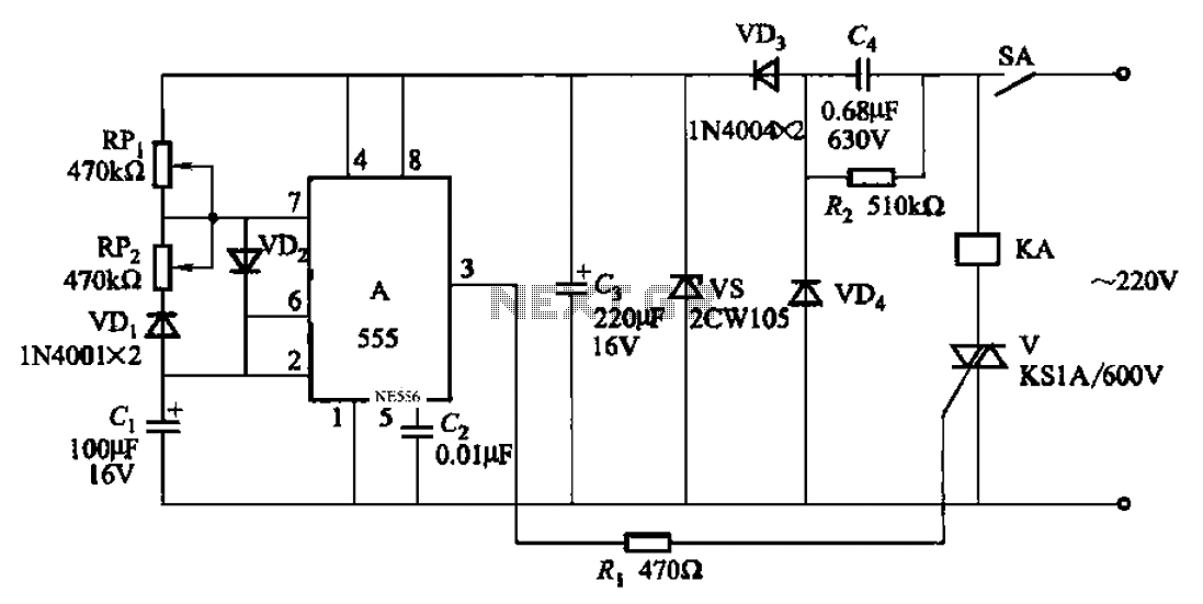
An automatic cycle switch circuit utilizing a 555 integrated circuit (IC) as the control element. It incorporates a capacitive step-down circuit and employs a bidirectional thyristor to control relays or loads with specific on and off timing. The circuit...

The controller for the Hybrid Power Plant (HPP) is represented in a block diagram format. It consists of 440 Wp photovoltaic modules, a 1 kW wind turbine, and a 5 kW diesel engine as a backup power source. The...
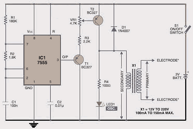
This is an electronic muscle stimulator circuit that stimulates the nerves in the area of the body where electrodes are attached. It is useful for relieving pain. The electronic muscle stimulator circuit operates by delivering electrical impulses through electrodes placed...
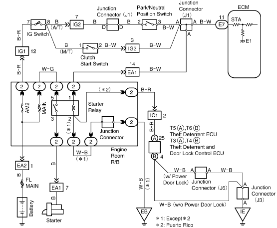
This document provides information regarding the wiring of the Toyota Tercel 1996. Component: intake air temperature sensor. The intake air temperature (IAT) sensor in the 1996 Toyota Tercel plays a crucial role in the vehicle's engine management system. It is...
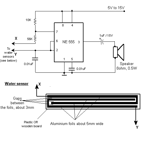
This circuit activates an alarm when its sensor comes into contact with water. It employs a 555 astable multivibrator that generates a tone of approximately 1 kHz upon water detection. The circuit consists of a 555 timer configured in astable...
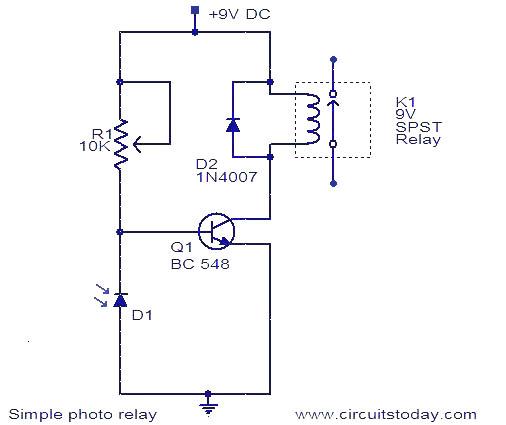
A photo relay, or light-activated relay, is a circuit that opens and closes relay contacts based on the presence of light. It utilizes a photodiode to detect light levels. The photodiode exhibits high resistance in the absence of light...