
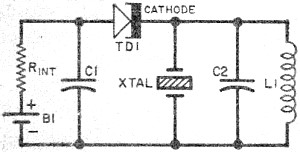
tunnel diode circuits
The forward characteristic curve of the tunnel diode illustrates this negative resistance region, where the current through the diode decreases even as the voltage across it increases. In comparison, a tetrode vacuum tube with a fixed screen voltage of 200 volts and a variable plate voltage between 0 and 300 volts demonstrates a similar behavior. As the plate voltage is increased, the plate current typically rises until it reaches around 100 volts, at which point a secondary emission from the plate causes the current to decrease. This decrease in plate current with an increase in plate voltage is another example of negative resistance. Once the plate voltage surpasses the screen voltage, the plate current resumes its increase. This behavior, contrary to Ohm's law, is characteristic of both the tetrode and the tunnel diode, which exhibit negative resistance in specific operating ranges.
The tunnel diode's unique properties make it suitable for various applications, particularly in high-speed electronics. Its ability to operate at high frequencies and its negative resistance characteristics allow for the design of oscillators, amplifiers, and other circuits that exploit these features. In practical circuit design, the tunnel diode can be integrated into oscillators to achieve stable frequency outputs, enabling advancements in telecommunications and signal processing technologies. The understanding of its operational principles and characteristics is crucial for engineers and designers working with high-frequency electronic systems.Leo Esaki invented the tunnel diode in 1957 while working at Sony (Tokyo Tsushin Kogyo at the time). Tunnel diodes have a very narrow, heavily doped p n junction only around 10nm (100 G…) wide that exhibits a broken bandgap, where conduction band electrons and therefore on the n-side are approximately aligned with valence band holes on the p-side facilitate the quantum mechanical tunneling process after which the diode is named. A negative differential resistance in part of their operating range makes them useful for high frequency oscillators. This article in a 1960 edition of Popular Electronics introduces the device`s characteristics and potential uses.
By now, just about everyone has heard of the tunnel diode, latest "miracle" from the semiconductor industry. Though related to the tube and transistor, the tunnel diode ordinarily has only two terminals. Yet it differs from other two-terminal devices (resistors, capacitors, and so on) in a very special way.
Apply voltage to a resistor, for example, and you can determine current flow by Ohm`s law. Increase the voltage across the resistor, and the current flow through the resistor will increase in proportion. But this is not so with the tunnel diode. The effect which brought about the practical construction of this unique semiconductor was discovered by Dr.
Leo Esaki, a brilliant Japanese scientist. Dr. Esaki determined that unusual doping of the germanium-diode junction would cause the current flow to decrease, even though the applied voltage was increased. This effect, known as negative resistance, enables the tunnel diode to perform its unusual feats. Fig. 2. Tunnel-diode forward characteristic curve. In negative-resistance slope range, current through diode decreases even though voltage across diode increases.
Figure 1(A) shows a tetrode vacuum tube with a fixed screen voltage of 200 volts and a plate voltage that can be varied between 0 and 300 volts. The tube`s control grid is grounded, since we need no input signal to the tetrode for the purposes of this example.
Let`s vary the plate voltage between 0 and 300 volts and record the changes in the tetrode`s plate current as shown on the milliammeter - see Fig. 1(B). Note that the plate current increases in the normal fashion as the plate voltage is increased until the plate voltage reaches a value of about 100 volts.
At this point a peculiar phenomenon occurs due to the secondary emission from the plate - the plate current decreases as the plate voltage increases. This decrease in plate current with increase in plate voltage is called negative resistance, which is a well-known characteristic of tetrodes.
When the plate voltage reaches the value of the screen voltage, 200 volts in this example, the plate current increases as before. Negative resistance is seemingly contrary to Ohm`s law. If we were to apply a steadily increasing voltage across a resistor, for example, the current through the resistor would increase proportionately.
If we carried this far enough, the resistor would eventually go up in smoke. But in this case, steadily increasing voltage on the tetrode`s plate brings steadily decreasing current. The tetrode in this example actually exhibits a negative resistance at plate voltages between about 100 and 200 volts.
Now that we know what negative resistance is, let`s return to the tunnel diode. The slope of the tunnel diode`s forward-characteristic curve is very much like the tetrode`s plate-characteristic curve. See Fig. 2. Note that as the diode voltage is increased positively from zero to Vp, the tunnel-diode curve is similar to that for any conven
🔗 External reference
Related Circuits
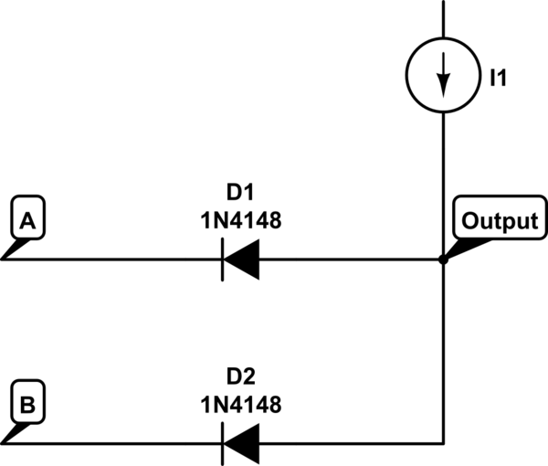
The voltage at the anode and cathode of the diodes is checked to determine whether they are conducting. There is confusion regarding the current source and how to determine the state of the diodes for input combinations (00, 01,...

Any standard oscillator, such as a Colpitts or Hartley configuration, can be utilized to generate the local oscillator (LO) frequency required by the NE602. The NE602 is a versatile integrated circuit commonly used in radio frequency applications, particularly in mixer...

This circuit is designed to test zener diodes. It connects to a 120V AC line and amplifies the output. The zener diode testing circuit operates by utilizing a transformer to step down the 120V AC line voltage to a more...
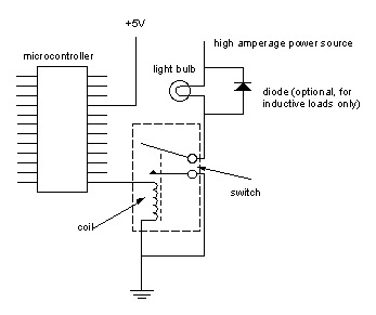
Digital output from a microcontroller is typically a low-amperage signal. For example, when a pin is set HIGH on the microcontroller (in Wiring/Arduino, it is digitalWrite(somePin, HIGH);), the voltage from that pin is usually +3.3V or +5V, with the...
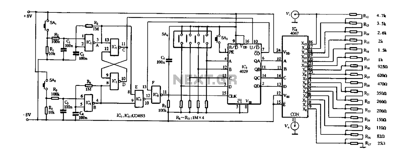
Figure 4-14 illustrates a digital integrated circuit featuring 16 preset potentiometers for Siniperca electronic circuits. The circuit comprises three main components: an input controller, a presettable counter, an analog electronic switch, and a resistor network. It includes a push-button...
Dark Activated Switch or Porch Light Switch. This circuit activates a relay when the light level drops below a preset threshold. The light sensitivity can be adjusted using variable resistor VR1, and the relay contacts can control an external...