
Closed-loop three-phase multivibrator
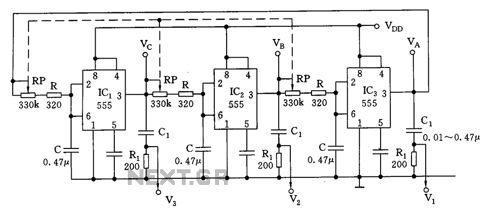
The circuit described features a closed-loop configuration of three identical Schmitt triggers, which serve as key elements in generating delayed output signals. Each Schmitt trigger flip-flop introduces a defined delay, calculated as td = (RP + R)C, where RP is the resistance associated with the charging path and R is an additional resistance in the circuit. The charging and discharging behavior of the capacitor C is critical for the timing characteristics of the entire circuit.
The rise time to achieve 1/3 of the supply voltage (VDD) is a significant parameter, as it establishes the responsiveness of the circuit during transitions. The 555 timer, a versatile component often used in timing applications, is reset to initiate the charging process of capacitor C through resistor R. The output from the third stage of the Schmitt trigger configuration (pin 3 of the IC) plays a crucial role in controlling the discharge path for the capacitor, effectively managing the time constant for charging and discharging cycles.
Each transition at the output of the flip-flop necessitates the engagement of three monostable trigger circuits, thereby amplifying the total time required for a complete output cycle. As a result, the overall output period (Td) is expressed as Td = 6td, indicating that the output signal's frequency is inversely proportional to this period. The design ensures that precise timing intervals can be achieved, making it suitable for applications that require controlled signal generation and timing management. This configuration is particularly advantageous in various electronic applications where timing accuracy is critical. As shown, this is a closed loop made up of three identical composition of the Schmitt trigger, end to end. Each flip-flop delay is td l. 1 (RP + R) C, i.e., the voltage on C td delay rise time required for the 1/3 VDD. The 555 is reset, the charge on C by R, W output end of the previous stage IC (3 feet) of sink current discharge, and thus the charging time constant C of the same. Thus, each output of the flip-flop every time you want to change through three monostable trigger circuit transmission, the time required is 3td.
Therefore, each IC output period Td 6td. The corresponding frequency
Related Circuits
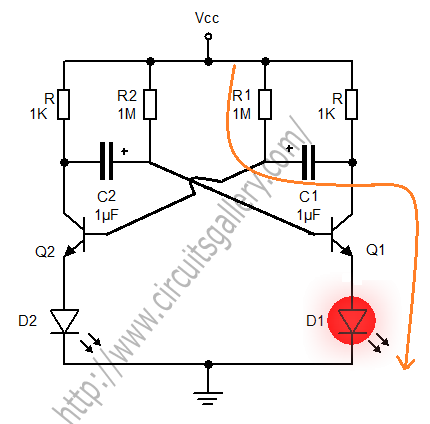
A transistorized astable multivibrator is a cross-coupled transistor network capable of generating a continuous square wave. It operates as a free-running oscillator or a regenerative switching circuit that utilizes positive feedback. The astable multivibrator continuously alternates between its two...

The capacitor C will charge through resistors Ra and Rb, and then discharge through resistor Rb only. The duty cycle may be controlled by the values of Ra and Rb. In this circuit configuration, a capacitor (C) is utilized to...
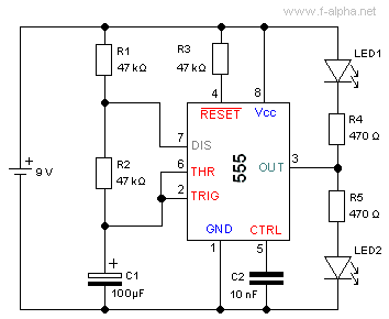
The NE555 can be used to construct an astable multivibrator or blinker. It is important to understand the necessary components and considerations involved in this process. The NE555 timer IC is a versatile device commonly used in various timing, pulse...
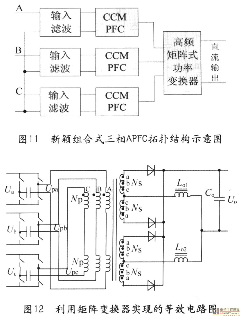
Tape isolate single-phase power factor correction (PFC) that utilizes DC/DC converters, consisting of two cables. The three-phase PFC is formed by connecting three single-phase PFCs in parallel at the output. This configuration is based on a matrix-type DC/DC converter...
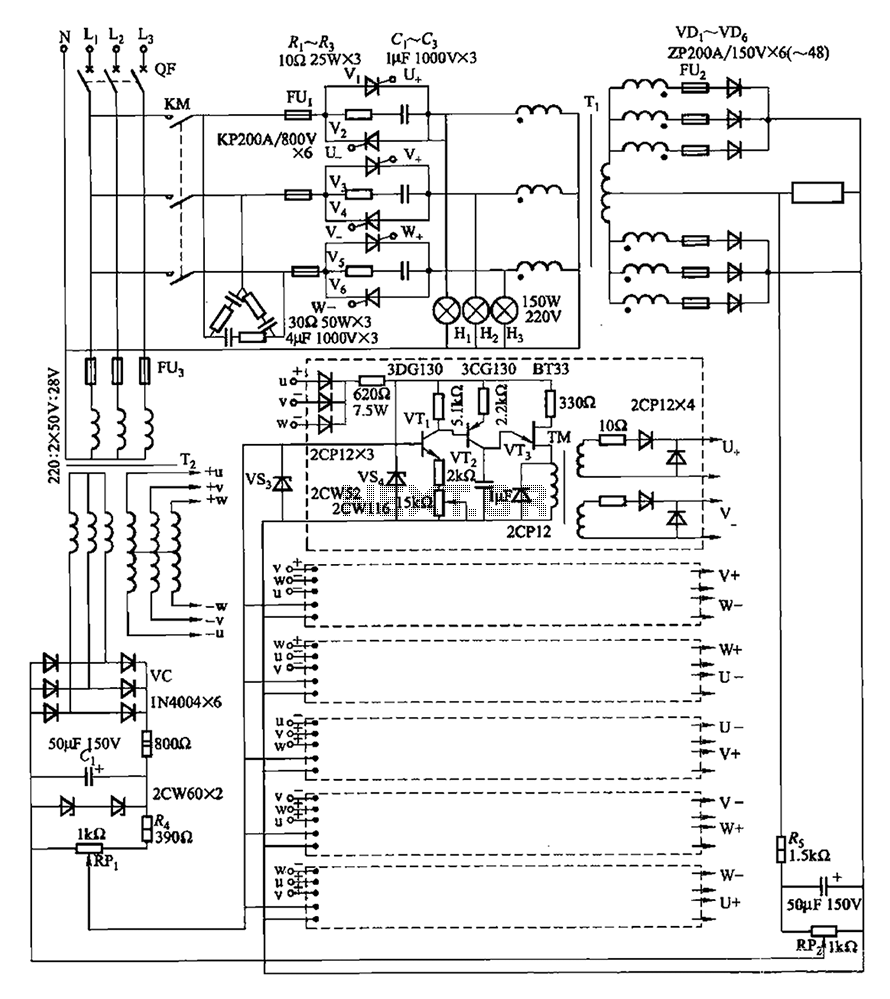
A three-phase thyristor power regulator circuit designed for plating applications, capable of handling currents from 1200A to 6000A at a voltage of 10V. The circuit comprises a main circuit, a trigger circuit, synchronous power components, and a voltage negative...
The semiconductor thermistor is an embedded thermal protection element that is sensitive to temperature, with a temperature error of 5 degrees. It offers reliability, a small size (diameter 3.5 mm), and ease of installation, making it suitable for embedding...