
Common-base Colpitts oscillator circuit

The common-base Colpitts oscillator is a robust circuit configuration known for its stability and frequency control capabilities. The PNP transistor acts as the core amplifying device, operating in a common-base mode, which is characterized by a low input impedance and high output impedance. This configuration is particularly advantageous for high-frequency applications, as it minimizes the Miller effect, allowing for better frequency response.
The tank circuit, composed of capacitors C1 and C2, plays a critical role in determining the oscillation frequency. The values of these capacitors can be finely tuned, enabling precise control over the output frequency of the oscillator. The interaction between the capacitors and the inductor in the tank circuit creates resonant conditions that are essential for sustained oscillation.
The feedback mechanism is crucial for the oscillator's operation. The regenerative feedback from C2 to the emitter enhances the transistor's conduction during specific intervals of the cycle, promoting oscillation. The relationship between the collector and emitter signals ensures that the feedback is always in phase, a necessary condition for stable oscillation.
During operation, as the emitter voltage fluctuates, the feedback loop continuously adjusts the transistor's biasing conditions, maintaining oscillation. The cycle of charging and discharging of C1 and C2, coupled with the magnetic field dynamics of transformer T1, creates a self-sustaining oscillation that can be harnessed for various applications, such as signal generation in RF communication systems.
The detailed understanding of this oscillator's operation allows for its application in various electronic devices where stable frequency generation is required, including oscillators for RF transmitters, signal generators, and waveform generators in testing and measurement equipment.A common-base Colpitts oscillator using a pnp transistor as the amplifying device. Notice in this version of the Colpitts oscillator that regenerative feedback is obtained from the tank circuit and applied to the emitter. Base bias is provided by resistor RB and RF. Resistor RC is the collector load resistor. Resistor RE develops the input signal and also acts as the emitter swamping resistor. The tuned circuit consists of C1 and C2 in parallel with the primary winding of transformer T1. The voltage developed across C2 is the feedback voltage. Either or both capacitors may be adjusted to control the frequency. In the common-base configuration there is no phase difference between the signal at the collector and the emitter signal. Therefore, the phase of the feedback signal does not have to be changed. When the emitter swings negative, the collector also swings negative and C2 charges negatively at the junction of C1 and C2.
This negative charge across C2 is fed back to the emitter. This increases the reverse bias on Q1. The collector of Q1 becomes more negative and C2 charges to a negative potential. This feedback effect continues until the collector of Q1 is unable to become any more negative. At that time the primary of T1 will act as a source because of normal tank circuit operation. As its field collapses, the tank potential will reverse and C1 and C2 will begin to discharge. As C2 becomes less negative, the reverse bias on Q1 decreases and its collector voltage swings in the positive direction. C1 and C2 will continue to discharge and then charge in a positive direction. This positive-going voltage across C2 will be fed back to the emitter as regenerative feedback. This will continue until the field around the primary of T1 collapses. At that time the collector of Q1 will be at a maximum positive value. C1 and C2 will begin to discharge and the potential at their junction will become less positive. This increases the reverse bias on Q1 and drives the collector negative, causing C1 and C2 to charge in a negative direction and to repeat the cycle.
🔗 External reference
Related Circuits
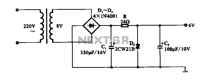
A DC shunt regulator power supply circuit is presented, which operates in parallel with a radio circuit. The circuit begins with an AC voltage of 22V, which is stepped down to 8V using a transformer. The 8V AC voltage...
This design outlines a simple 1 kHz square wave generator utilizing a few components and the LM3909 integrated circuit, which is beneficial for testing audio equipment. The circuit operates on a single 1.5V battery cell, producing a maximum output...
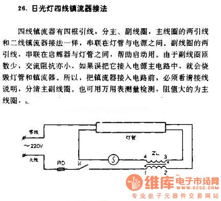
The four-wire ballast connection of a fluorescent lamp consists of four lead wires, which include main and auxiliary coils. The connection of the two lead wires in the main coil is similar to that of a second-line ballast; both...
The circuit involves a Signetic balance modem connection utilizing a transistor array as a phase detector. It provides information about the cosine of the phase angle, which corresponds to the frequency of the input signal combined with the integrated...
This AC to DC power supply can output 5A in continuous operation and 12A peak current. This type of DC power supply uses a PCB, allowing for two case types. The described AC to DC power supply is designed to...
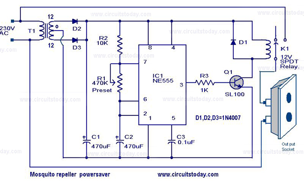
The circuit diagram of a mosquito repellent power saver circuit is provided along with a detailed explanation. The mosquito repellent power saver circuit is designed to efficiently operate a mosquito repellent device while minimizing energy consumption. This circuit typically integrates...