
Controlled Transistor Series Regulator With Overload and Short-Circuit Protection
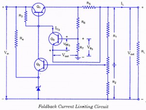
The described circuit functions as a robust current limiting mechanism to protect the components from excessive load currents. The inclusion of the foldback current limiting circuit enhances the reliability of the voltage regulator by reducing the power dissipation across the pass transistor during fault conditions. The voltage divider network, which biases transistor Q3, plays a critical role in ensuring that the base voltage is adequately controlled, enabling timely activation of the current limiting feature. This design is essential in applications where load conditions may fluctuate, ensuring that the circuit can handle unexpected changes without compromising component integrity. The careful selection of resistor values and the characteristics of the transistors involved are crucial for achieving the desired performance and protection levels in the system.If the load resistance RL is reduced or load terminals are shorted acciden tally, a very large load current will flow. It may destroy the pass transistor Q1, diode or possibly some other component. Fuse protection will not prove adequate because the transistor may get damaged in a very small fraction of a second The current limit ing circuit con
sists of a transistor Q3 and a re sistor R5 (approxi mately 1 ohm) connected between base and emitter terminals of transistor Q3. With normal load current, transistor Q3 remains off because the voltage drop across resistor R5 is small (less than about 0.
7 V necessary for making the transistor Q3 on). Under this condition, the circuit works normally, as described above. With the excessive load current (exceeding 0. 6/1, that is, 0. 6 A or 600 mA) the voltage drop across R5 becomes large enough to turn transistor Q3 on. The collector current of transistor Q3 flows through R3 thereby decreasing the base voltage of transistor Q1. This results in reduction of the conduction level of transistor Q1. Thus further increase in load current is prevented. Figure summarizes the current limiting. When load resistance RL is infinite, the output voltage is regulated and has a value of VREQ. The load current IL is zero for this operating condition. When RL decreases, the load current IL increases upto the point where RL becomes equal to RL(min) At this minimum load resist ance, IL equals 600mA and VBE equals 0.
6V. Beyond this point, transistor Q3 turns on and the current limiting sets in. Further decrease in RL produces decrease input voltage, and regulation is lost. When RL is zero, the load current IL is limited to a value between 600 m A and 700 m A. The load current with shorted-load terminals is symbolized as ISL. When the load terminals are shorted in fig. 30. 9, the volt age across resistor R5 is The simple current limiting circuit also has a drawback of large power dissipation across the series pass transistor. With a short across the load, almost all the input voltage appears across the pass transistor. So the pass transistor has to dissipate approximately A problem with the simple current limiting circuit just discussed is that there is a large amount of power dissipation in series pass transistor Q1 while the regulator remains short-circuited.
The foldback current limiting circuit is the solution of above problem. The circuit of a transistor series voltage regulator with foldback current limiting facility is illustrated in the figure. In this circuit base of transistor Q3 is biased by a voltage divider network consisting of resistors R6 and R7.
The load current IL flows through resistor R5, causing a voltage drop of IlR5(approximately) across it. Thus a voltage of (IlR5 + Vout) acts across the voltage divider (R6 R7) network. The voltage applied to the base of transistor Q3 is equal to the voltage drop across resistor R7 and is given as Thus the magnitude of base drive of transistor Q1 is by this Vbe3.
Now if load resistance decreases, may be due to any reason, load current IL will increase causing voltage drop Il, R5 to increase. This causes VB3 to increase and therefore Vbe3 to increase. This makes transistor Q3 on in a stronger way. The increased collector current Ic3 of transistor Q3 flows through the resistor R3 thereby decreasing the base voltage of transistor Q1 This results in reduction of the conduction level of transistor Q1.
Thus further increase in load current is prevented. From the equations above it is obvious that VBE in this circuit is much more than that was in circuit illustrated in the above figure(only ILR5). It means that the increment in load current is limited by larger amount in circuit shown in figure. Due to reduction in load resistance RL, VBE3 increases to a level so that transistor Q3 gets saturated.
Now collector current Ic3 becomes constant. Any further decrease in RL will have no effect on 🔗 External reference
Related Circuits
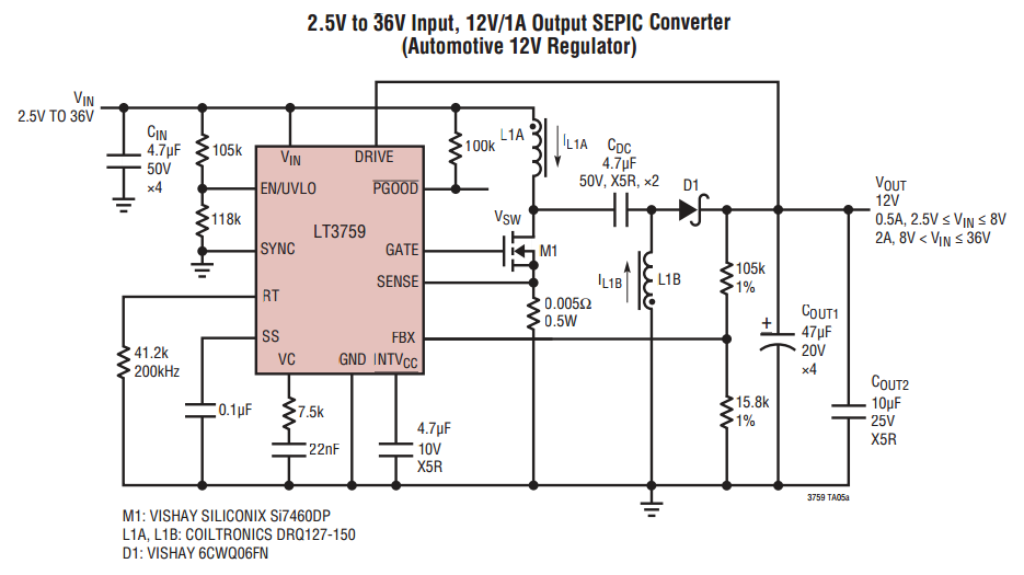
When VOUT is very low during startup or in the event of a short-circuit fault at the output, the switching regulator must operate at low duty cycles to keep the power switch current within the current limit range. This...
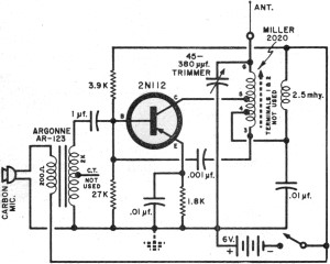
It had been a little over a decade since the invention of the transistor when this article appeared in the August 1959 edition of Popular Electronics. Transistors were still a mystery to many, including engineers, technicians, and hobbyists. Author...
The schematic represents a relatively simple transistor circuit. Analyzing such schematics evokes memories of college days spent studying electrical engineering. However, the complexity of the schematic can be daunting after a long time away from the subject. To refresh...

In telecommunications, Frequency Modulation (FM) transmits information over a carrier wave by varying its frequency. FM is widely utilized at VHF radio frequencies for high-fidelity broadcasts of music and speech. The global broadcast band is situated within the VHF...
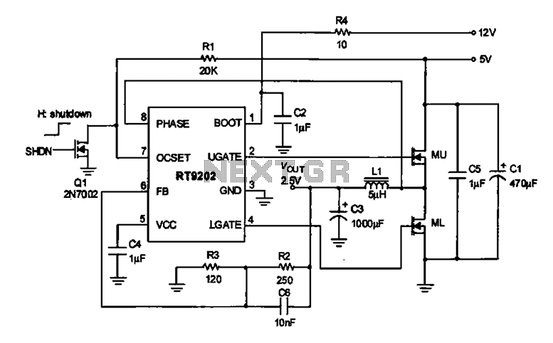
A 2.5V voltage regulator circuit is illustrated, which is part of a computer's motherboard. The circuit employs an oscillation circuit with the RT9202 control core chip, converting a 5V input supply into a regulated +2.5V output voltage, with the...
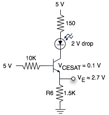
When building amplifiers, it is often necessary to test transistors, either to verify that they (still) work, or for some esoteric designs it may even be necessary to match certain characteristics. The design featured here is just what you...
Warning: include(partials/cookie-banner.php): Failed to open stream: Permission denied in /var/www/html/nextgr/view-circuit.php on line 713
Warning: include(): Failed opening 'partials/cookie-banner.php' for inclusion (include_path='.:/usr/share/php') in /var/www/html/nextgr/view-circuit.php on line 713