
Cosimulation with Analog-RF Systems

For designs of low complexity, it is possible to use separate simulators for the signal processing and analog/RF portions and then integrate the results. However, today`s state-of-the-art designs using a mix of analog/RF and dedicated on-chip DSP blocks require high levels of integration at the two-environment boundary.
Advanced Design System cosimulation between signal processing and circuits addresses this need. ADS Ptolemy provides the signal processing simulation, while the analog/RF simulation is provided by either the Circuit Envelope or High-Frequency SPICE (Transient) simulators. Other types of cosimulation include placing MATLAB components or HDL blocks in a signal processing simulation.
This topic describes cosimulation with analog/RF systems. For information on A/RF cosimulation with Cadence refer to the Cadence Library Integration documentation. For specific details, see Running a DSP and Analog - RF Cosimulation with RFIC Dynamic Link. The following figure shows a mixture of RF circuitry and DSP components. ADS provides a variety of analog/RF circuit simulators, including Linear, Harmonic Balance, Circuit Envelope, High-Frequency SPICE, and Convolution.
For signal processing simulation, ADS Ptolemy is used. Only circuits simulated with either Circuit Envelope or High-Frequency SPICE can be instantiated as a subnetwork and included in a signal processing schematic. These circuit blocks can then be simulated along with signal processing components. The steps needed for cosimulation are described in the next section. In the analog/RF circuit Schematic window, create a circuit schematic that includes a simulation component for either Circuit Envelope (called ENV) or High-Frequency SPICE simulation (called TRAN).
In the previous figure, a diode rectifier is set to be simulated with the Circuit Envelope simulator. Next, we will place this subnetwork in the signal processing schematic where it will be represented as a block.
To place the circuit subnetwork(s) you have already created in the signal processing schematic, choose Component > Component Library. Your opened projects are listed at the top of the list. Circuit projects have (A/RF) at the end. As stated earlier, ADS Ptolemy can cosimulate with only the Circuit Envelope or High-Frequency SPICE simulators.
Any circuit simulation control components other than ENV or TRAN (such as for harmonic balance or S-parameter simulation) are ignored in the cosimulation from the signal processing schematic. Both Circuit Envelope and Transient simulators deal with time-domain signals. Therefore, signal processing components connected to the circuit subnetwork must be the timed type. If the input component (connecting signal processing components to the circuit) produces numeric data, place an appropriate numeric-to-timed converter (such as float-to-timed or complex-to-timed) in your schematic.
These components (located in the Signal Converters library) ensure that the input into the circuit subnetwork is in the time domain. Refer to Time Converters for more information. Automatic Verification Modeling is a simulation mode that can significantly accelerate formerly lengthy cosimulations of Analog/RF circuits.
You can enable Automatic Verification Modeling in the Circuit Envelope Simulation Controller. When enabled, this mode characterizes an analog subcircuit into a behavior model, then the model is used to predict the response of the subcircuit at each time point. For details about Automatic Verification Modeling, see Automatic Verification Modeling. On UNIX platforms, you must copy an example project to a directory for which you have write permission.
On Windows platforms, you can work directly in the Examples directories; however, it`s better to copy examples to a working directory. In the To Project area, click Startup Directory or Working Directory to select the destination directory for the copied project.
Click Browse to select another directory. In the ADS Main window, choose File > Open Project to open the Open Project dialog box. In the Directories list, select the directory to which you copied the example. In the DUT_Mixer, double-click the Envelope simulation controller to open its setup dialog. Select the Cosim tab, and click Enable AVM (Fast Cosim) to enable the mode. To enable AVM (Fast Cosim) directly on the schematic, click the Display tab on the Circuit Envelope setup dialog. Enable the ABM_Mode parameter. On the schematic, set ABM_Mode=yes to enable the mode; set ABM_Mode=no to disable the mode. Clustering is the process of defining the boundaries of the signal processing and analog/RF simulators.
Initially, this boundary is defined by circuit schematics, where you define the circuit subnetworks and then make an instance of those on the Signal Processing schematic. However, there is a bit more to clustering than what is on the two schematics. Circuit subnetworks directly connected in the Signal Processing schematic are automatically clustered and treated as one circuit subnetwork, as shown in the following figure.
Therefore, use only one circuit simulation control component in either of the two (or more) directly connected subnetworks. When two circuit subnetworks defined on two different circuit schematics are connected on a Signal Processing schematic, the two circuit subnetworks are clustered into one (this is done transparently and should not concern the user).
However, if each of these two circuit subnetworks use their own simulation controller, then the circuit engine would not know which one to choose for simulation and would result in an error message. Another aspect of clustering is when circuit components available on the Signal Processing schematic (resistors in the first release of Advanced Design System) are connected to a circuit subnetwork.
In this case, such resistors will be absorbed into the circuit subnetwork during the clustering and will be simulated by the circuit engine as part of circuit subnetwork. Circuit subnetworks that form a feedback loop via signal processing components require a delay component in the feedback loop to facilitate the signal processing simulation scheduling, as shown in the following two figures.
If such a delay is not present, an error message will be issued. To have the program automatically insert the delay, you must edit the DF (data flow) controller parameters. To do this, double-click the controller, choose the Options tab, then eq parameter. 🔗 External reference
Related Circuits
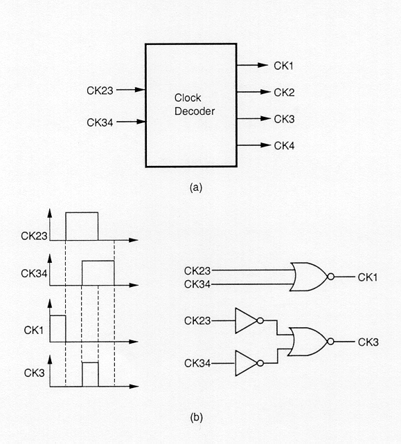
Clock signals are essential for digital systems, and their stability is crucial. Ideally, clock signals should exhibit minimal rise and fall times, specified duty cycles, and zero skew. However, in practice, clock signals often have non-zero skews, noticeable rise...
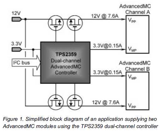
The new TPS2359 hot-plug controller integrates all power management functions for two AdvancedMC (AMC) modules. Its current limiting circuitry enables designers to meet stringent AMC requirements, particularly in applications utilizing redundant supplies. A unique feature called multiswap maintains a...
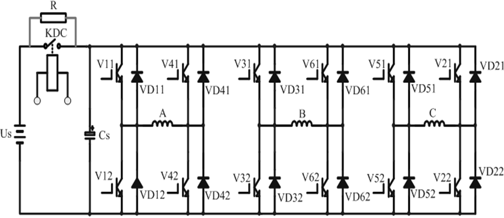
With the continuous growth of global vehicle production and ownership, the problems associated with vehicles are becoming increasingly apparent, particularly in China. Consequently, the development of zero-emission electric vehicles has emerged as a primary scientific research focus for many...
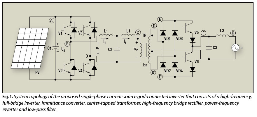
The electric utility grid-connected photovoltaic (PV) system is a significant technology for future renewable energy applications. The electric utility grid-connected photovoltaic (PV) system plays a crucial role in the advancement of renewable energy technologies. This system integrates solar panels into...

The design of solar panel systems with a lead-acid buffer battery is typically configured to ensure that the battery remains charged even during periods of limited sunlight. Solar panel systems integrated with lead-acid buffer batteries are designed to optimize energy...
The mine railway connects the national railways and intermediate links of the mining area, serving as an important component of the railway transport network. Statistics indicate that the Chinese mine railway extends over 20,000 kilometers, with numerous road junctions...