
Crystal oscillator circuit diagram of a compatible IC
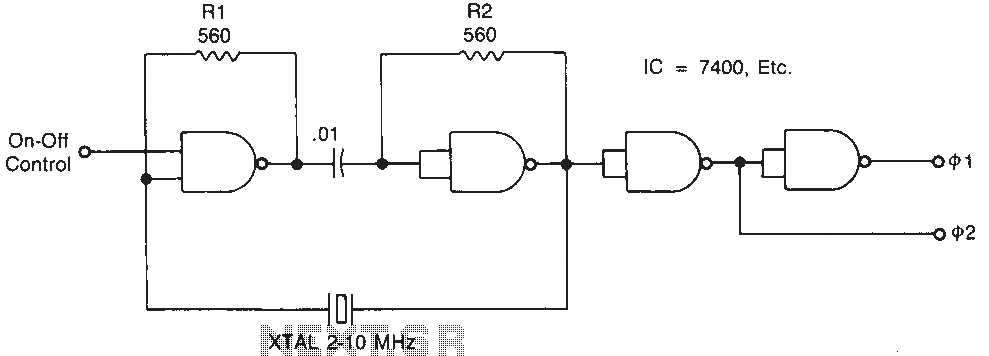
The described circuit configuration utilizes temperature-stable resistors R1 and R2, which are critical for maintaining consistent performance across varying thermal conditions. These resistors are integral to the NAND gate logic, ensuring that the output remains stable and predictable when the input conditions are met. The linear operation of the switches is crucial for minimizing distortion and ensuring that the circuit operates efficiently.
Capacitor C1 serves a dual purpose in this configuration. It acts as a coupling capacitor that filters out AC components while allowing DC signals to pass through, which is essential for maintaining the integrity of the signal at the operational frequencies. The specification that the impedance must be less than 0.1 ohm indicates a focus on minimizing losses and ensuring that the circuit can respond quickly to changes in input signals.
The circuit's operation in resonant mode suggests that it is designed to take advantage of the natural oscillations within the system, likely enhancing the gain and efficiency of the transistor. The inclusion of a series transistor with low series resistance is vital for achieving high-frequency performance, as it reduces the voltage drop across the transistor and allows for better signal fidelity.
The use of the AT cut method for the transistor is particularly noteworthy, as it allows for stable frequency performance within the range of 1-10 MHz. This method involves cutting the crystal at a specific angle to optimize its frequency response, making it suitable for applications requiring precise timing and frequency stability. Overall, this circuit design reflects a careful consideration of component selection and configuration to achieve reliable operation in high-frequency applications.Temperature stable resistors R1 and R2 NAND gates, they ensure that the switches in the linear region open. Capacitor C1 is a DC component at the operating frequencies, the impedance must be less than 0.1 ohm. It runs in a resonant mode transistor in series. Its series resistance is low, transistor AT cut method also can work within 1-10MHz range.
Related Circuits
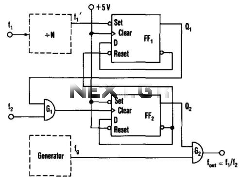
This circuit generates an output frequency that is linearly proportional to the ratio of two input frequencies. Each pulse of the bias frequency will open a switch for a period equal to half of the second input frequency, allowing...
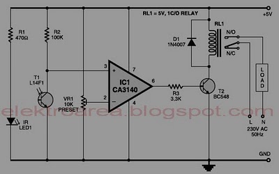
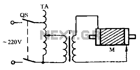
Typically, home appliances are controlled using switches, sensors, and similar devices. However, physical interaction with switches can pose safety risks in the event of a short circuit. The circuit outlined here eliminates the need for physical contact to operate...

This is a design circuit diagram of a versatile FM transmitter. This circuit does not include a coil and is simple and easy to assemble. It operates based on gate logic concepts. The circuit features a buffer gate N1...
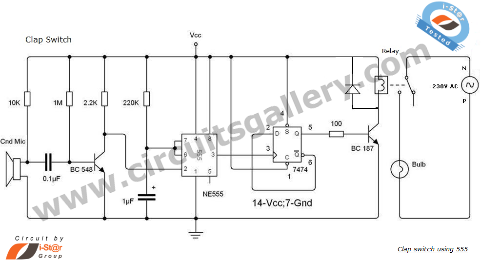
This is an intriguing 555 timer circuit designed to entertain and engage individuals while studying electronics in educational settings. Commonly referred to as a clap switch circuit, it operates as a sound-controlled flip-flop. This sound-controlled light can also function...
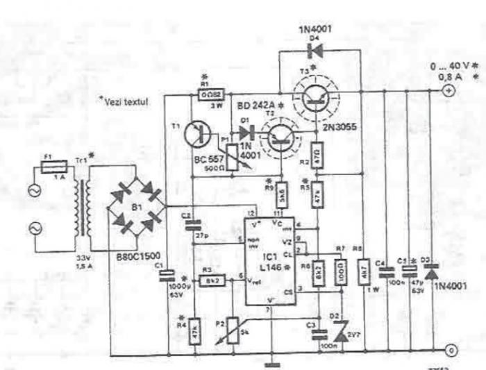
An adjustable laboratory power supply capable of providing an output voltage range from 0 to 60 volts can be constructed using the provided circuit diagram. This power supply can utilize the LM723 chip for lower voltage applications or, for...
Check the three-phase motor with broken bars as shown in the inspection circuit for the three-phase motor with broken bars. The inspection circuit for a three-phase motor with broken bars is designed to diagnose and evaluate the condition of the...