
cut the feed forward in the miller compensation with voltage buffer
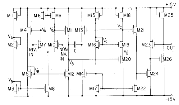
The operational amplifier described is a sophisticated circuit designed for high performance and stability, utilizing advanced MOS technology. The n-channel Al-gate MOS fabrication process allows for enhanced performance characteristics, particularly in terms of speed and power efficiency. The source-coupled differential amplifier at the input stage is crucial for achieving high common-mode rejection and low noise, which are essential for precision applications.
The differential-to-single-ended converter plays a vital role in transforming the differential output into a single-ended signal suitable for further processing. This conversion is critical in applications where a single-ended output is required, such as in many analog signal processing tasks. The cascode stage enhances the amplifier's output impedance, improving the overall gain and bandwidth of the amplifier.
The implementation of a Miller compensation scheme is a key aspect of maintaining stability across the operational amplifier's frequency response. By using a capacitor to create a dominant pole, the circuit can effectively manage gain and phase characteristics, ensuring that the amplifier remains stable under varying load conditions. The careful design choice to avoid direct connection of the compensation capacitor between the input and output of the cascode stage is a strategic decision to prevent the introduction of undesirable phase shifts that could compromise the amplifier's performance.
The addition of a source follower as a buffer in series with the compensation capacitor is an innovative solution to eliminate the right-half plane zero. This design choice not only maintains the integrity of the feedback loop but also enhances the overall frequency response of the amplifier, allowing it to perform optimally across a wide range of frequencies.
Overall, the operational amplifier's design reflects a thorough understanding of electronic circuit principles, ensuring that it can deliver high performance in demanding applications while maintaining robustness against variations in manufacturing processes. The schematic, as illustrated, provides a clear representation of the operational amplifier's architecture, highlighting the interconnections and functional blocks that contribute to its performance.An internally compensated operational amplifier is described which has been fabricated using n-channel Al-gate MOS technology. Only enhancement mode devices are used, and the circuit has been designed so that its performance is insensitive to process parameters.
A block diagram of the operational amplifier is shown in Fig. 1. The input stage is a source-coupled differential amplifier. The differential output signal of this stage is applied to a differential-to-single-ended converter, which develops a single-ended version of that signal. The converter drives a cascode stage, around which feedback is applied through a source follower and a capacitor, to implement a Miller compensation scheme.
Another source follower, fed from the cascode stage, drives the output stage. The bias point interdependence of the stages is such that their quiescent voltages track one another, so that all stages except the last two remain Frequency compensation of the circuit is accomplished through the capacitance C, shown in Fig. 1, which is Miller multiplied by the cascode stage and used to create a dominant pole in conjunction with the output resistance of the differential-to-single-ended converter.
The compensation capacitor C is not connected directly between the input and output of the cascode stage because for an inverting gain stage with simple pole splitting compensation, the compensation capacitor, in addition to introducing a dominant pole, also introduces a right half plane zero corresponding to ‰z = gm/C, where gm is the transconductance of the stage and C the compensation capacitance. The right-half plane zero is clearly undesirable, since it degrades the phase of the complete amplifier by 90 ° at high frequencies, while at the same time eliminating the effect of the dominant pole on the gain magnitude frequency response by stopping the 20 dB/decade rolloff created by it.
For the values of C required and for the values of gm that can be achieved, the frequency of the zero is lower than that of the crossover frequency and thus frequency compensation becomes impossible. Physically, the zero is caused by feed-forward through the compensation capacitor. To eliminate this feed forward, a buffer implemented by a source follower is placed in series with C, thus preventing the feedforward and therefore eliminating the right-half plane zero, while at the same time allowing feedback which gives rise to the desirable dominant pole.
The complete amplifier schematic is shown in the figure below. 🔗 External reference
Related Circuits
This simple amplifier is ideal for adding a headphone jack to equipment that lacks this feature. The Headphone Buffer circuit board is small enough (1.2" X 1.4") to squeeze into even the smallest spaces and power requirements are so...
This device is designed to be a simple, inexpensive comparator intended for use in a solar cell power supply setup where a quick indication of "too low" or "just right" voltage is needed. The circuit consists of one 5V...
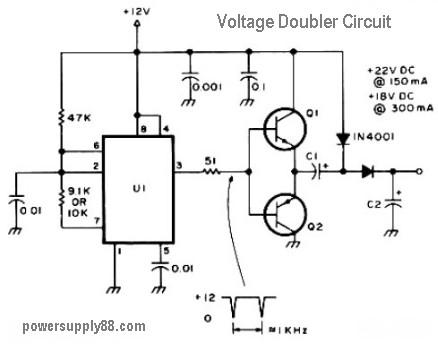
This circuit diagram represents a DC voltage doubler and DC converter. It is designed to convert a 12V DC power supply into outputs of 24V DC and 18V DC. Nearly any PNP or NPN power transistors can be utilized...

The UCD90124/A is utilized to monitor multiple voltages, some of which exceed 2.5V. Scaling circuits are implemented to prevent exceeding the 2.5V maximum on the MON inputs. The inquiry pertains to whether raw voltage values or scaled values should...
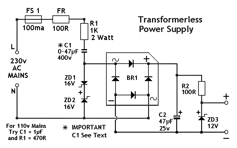
The circuit diagram was designed to create a power supply without utilizing any transformer circuit. This circuit illustrates the advantages as well as the limitations of transformerless power supplies. The transformerless power supply circuit typically employs a capacitive dropper method...
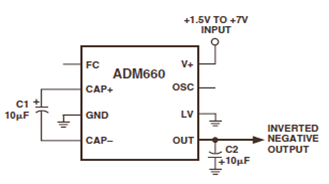
The ADM660 is a charge-pump voltage converter that can either invert the input supply voltage or double it. The schematic below depicts the ADM660 Voltage Inverter Circuit Configuration Diagram. This inverting schematic is ideal for generating a negative rail...