
Data Acquisition System I
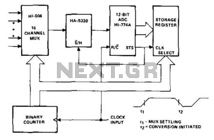
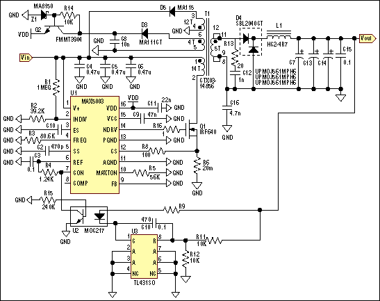
The HI-506 multiplexer is designed for efficient analog signal routing, enabling the selection of multiple input channels based on binary-coded inputs. This device is particularly useful in applications requiring rapid switching between analog signals, such as in data acquisition systems. The integration of the HA-5330 sample and hold circuit enhances the system's performance by capturing and maintaining the voltage level of the selected input during the analog-to-digital conversion process.
The control logic of the system is crucial for ensuring that the timing relationships between the multiplexer, sample and hold circuit, and the analog-to-digital converter (ADC) are maintained. The connection between the sample and hold control and the STS output of the HI-774A ensures that the sample and hold circuit only updates its output when a conversion is actively taking place. This prevents any erroneous readings that could occur if the input signal were to change during the conversion process.
The specified clock timings are critical to the operation of the system. The low duration of the clock signal must be carefully managed to ensure that the multiplexer can select the next channel while the ADC processes the current input. The timing constraints also guarantee that the T/C signal provides valid data at the correct moment, facilitating seamless data transfer into the storage register.
In scenarios where the incremented register address may lead to complications, the introduction of a 4-bit latch can effectively manage the address offset, ensuring that the data is accurately recorded in the intended register. This additional component can help maintain data integrity and simplify the overall design by allowing for flexible addressing options.
With a clock frequency of 100 kHz, the system is capable of reading each channel every 160 µs, making it suitable for applications that require moderate-speed sampling of multiple analog signals. This operational speed, combined with the effective control logic and signal routing capabilities, positions the HI-506 multiplexer and associated components as a robust solution for analog signal processing tasks in various electronic applications. The HI-506 multiplexer is used as an analog input selector, controlled by a binary counter to address the appropr iate channel. The HA-5330 is a high-speed sample and hold. The sample/hold con- trol is tied to the status (STS) output of the HI-774A; whenever a conversion is in process, the S/H is in the hold mode. A conversion is initiated when the clock input becomes low; when the clock becomes high, the mux address changes.
The mux will be acquiring the next channel while the ADC is converting the present input, held by the S/H. The clock low time should be between 225 ns and 6.5 jus, with the period greater than 8.5 $. With this timing, T/C will be high at the end of a conversion, so the output data will be valid - 100 ns before STS goes low.
This allows STS to clock the data into the storage register. The register address will be offset by one; if this is a problem, a 4-bit latch can be added to the input of the storage register. With a 100-kHz clock rate, each channel will be read every 160us. 🔗 External reference
Related Circuits
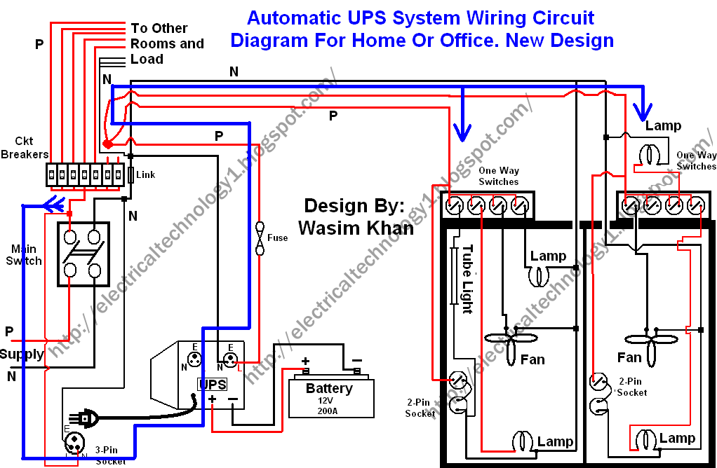
This wiring circuit diagram is designed for providing power to specific rooms in a home or office during a power supply failure. It ensures continuous power supply to devices such as laptops and computers in those particular rooms, especially...
This page serves as documentation for the circuits built utilizing the Modular Signal System, initially documented by Gregg Fuhriman in Railmodel Journal and further detailed on the Free-mo.org website. This project involved designing and constructing a circuit board for...
Nowadays every institution needs automation. As a part of college automation, a project has been developed for a Voice Interactive System for College Automation. This project allows users to quickly access student attendance and marks through the telephone line...
A 50W isolated forward-converter switching supply for telecom applications is described. Most aspects of the design are discussed. The 50W isolated forward-converter switching supply is engineered to meet the specific demands of telecom applications, where reliability and efficiency are paramount....
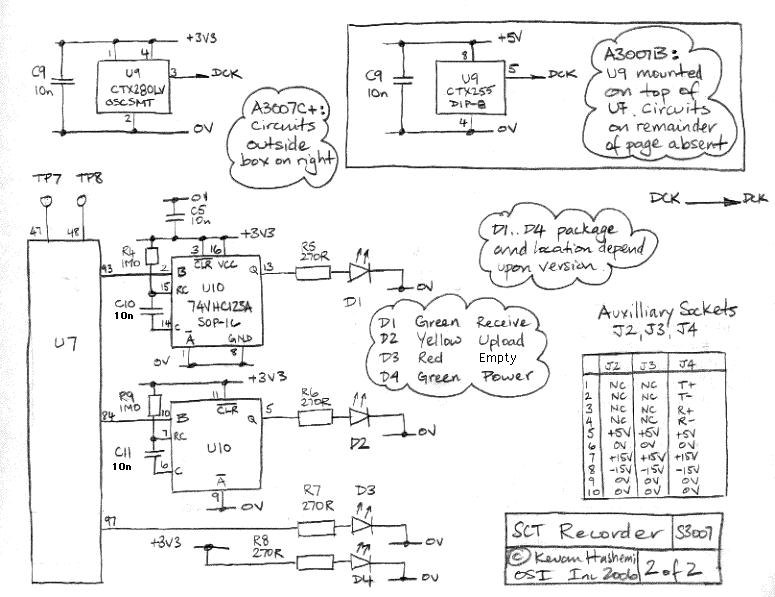
The Data Recorder (A3007) is a LWDAQ device that decodes and records subcutaneous transmitter (SCT) messages. The A3007 processes the signal generated by a demodulator, such as the Demodulating Amplifier (A3017), to identify valid SCT message sequences. It stores...
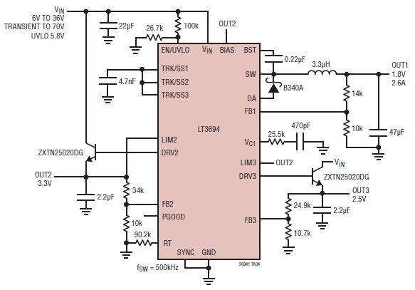
The LT3694 is a monolithic, current mode DC-DC converter that can be designed as a simple step-down converter, supporting a maximum output current of 2.6 A. This switching step-down converter is capable of generating up to 2.6 A at...