
DC-coupled multi-stage amplifier circuit a
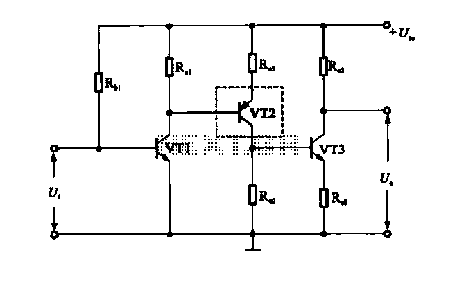
The multi-stage DC-coupled amplifier circuit is designed to provide significant amplification while maintaining stability and linearity across its operational range. The use of NPN transistors in the initial stages allows for efficient amplification of the input signal. Each stage is configured to ensure that the biasing conditions are optimized, allowing the amplifier to operate effectively without distortion.
As the signal progresses through each stage, the collector potential incrementally rises. However, this increase in potential can lead to a reduction in the overall output voltage range, which may limit the circuit's performance in certain applications. To mitigate this effect, the implementation of PNP transistors in conjunction with NPN transistors is a common practice. The PNP transistor (VT2) can effectively lower the DC potential of the subsequent stage (VT3), allowing for a more manageable output voltage range.
In addition to using complementary transistor configurations, the circuit can also incorporate an emitter follower stage. This configuration serves as a buffer that provides voltage gain while simultaneously reducing the DC potential seen by the following stages. The emitter follower is characterized by its high input impedance and low output impedance, making it an ideal choice for interfacing between stages of an amplifier.
In summary, the multi-stage DC-coupled amplifier circuit leverages the properties of both NPN and PNP transistors to achieve a robust amplification solution, while the inclusion of emitter follower stages enhances the circuit's overall performance by managing DC levels effectively.DC-coupled multi-stage amplifier circuit a (3) multi-stage DC-coupled amplifier in DC-coupled by a multi-stage amplifier circuit amplifying circuit, if used NPN type transistor of each stage, in order to fit all levels have appropriate operating point of stage base, Step by step the collector potential increases, so reducing the final output voltage range. In order to solve this problem, in practice, it can be used in conjunction with NPN and PNP transistor to reduce the post-stage DC potential, as shown in FIG.
Figure (8) shows an NPN cvri) and PNP transistor (VT2) wish, is used to reduce the subsequent stage (VT3) potential. Alternatively, you can use emitter follower, stage amplified voltage diode to reduce a DC potential of the circuit.
Figure l-43 (b) shows the use of emitter cvn) is used to reduce the subsequent stage (, rr3) potential.
Related Circuits
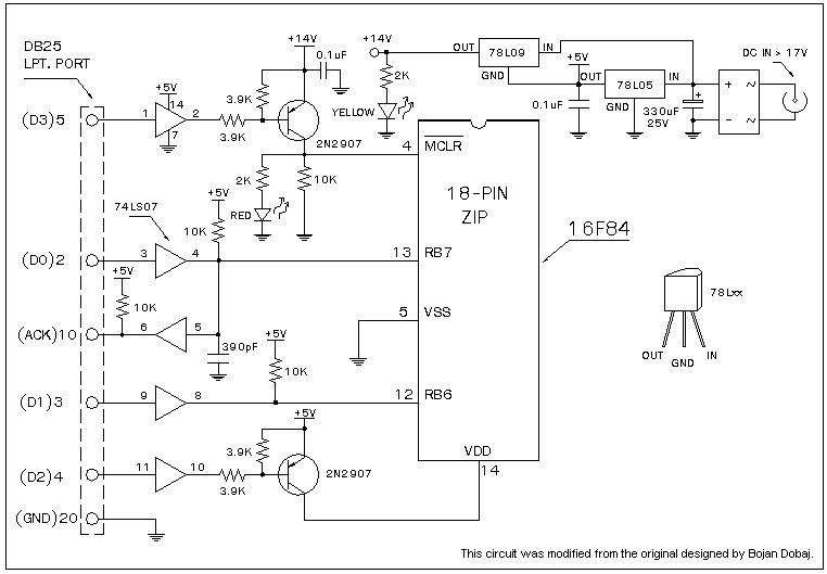
A universal Windows-based software designed to work with any serial programmers for the PIC16F84, known as WPicProg16 V1.20. It is recommended to build this programmer before starting various interesting projects with the F84. Some PIC programmers support in-circuit programming,...
Excellent Joule thief circuit idea! The Joule Thief is a simple yet effective circuit designed to extract usable voltage from low-voltage power sources, such as depleted batteries. This circuit operates on the principle of boosting voltage through the use...
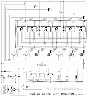
The MM5314 is a monolithic MOS integrated circuit that incorporates P-channel low threshold enhancement mode and ion implanted depletion mode devices. It features an internal multiplex oscillator, fast and slow set controls, a single power supply, 7-segment outputs, leading...
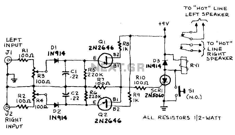
The circuit input is derived from the terminal loudspeaker or amplifier output jacks. If the right channel signal is sufficiently strong to charge capacitor C1 to a potential that exceeds the breakdown voltage of the emitter of transistor Q1,...
Pressing the pushbutton on the transmitter activates a sound and/or light alert in the receiver. This system operates without wiring or radio frequencies; instead, the transmitted signal is conveyed through the mains supply line. It is suitable for use...
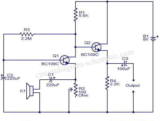
This circuit diagram illustrates the conversion of a speaker into a microphone. When sound waves impact the diaphragm of a speaker, fluctuations occur in the coil, generating an induced voltage. This induced voltage is typically substantial but low in...
Warning: include(partials/cookie-banner.php): Failed to open stream: Permission denied in /var/www/html/nextgr/view-circuit.php on line 713
Warning: include(): Failed opening 'partials/cookie-banner.php' for inclusion (include_path='.:/usr/share/php') in /var/www/html/nextgr/view-circuit.php on line 713