
DC DC Converter From 1 5V To 34V
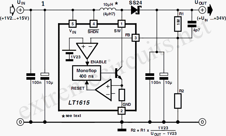
The LT1615 step-up switching voltage regulator is designed for efficiency and versatility in various applications, including powering LCD screens and providing biasing for RF circuits. Its ability to generate a high output voltage from low input voltages makes it particularly useful in battery-powered devices. The compact SOT23 package allows for integration into space-constrained designs, making it suitable for portable electronics.
In practical applications, careful attention must be paid to the layout and component selection to ensure optimal performance. The use of low-ESR capacitors at the input and output is critical to minimize voltage ripple and enhance transient response. The choice of inductor affects not only the efficiency but also the output voltage stability; therefore, selecting the appropriate inductor value based on the desired output voltage is essential.
The feedback loop's design, including the selection of resistors R1 and R2, should be optimized to achieve the desired output voltage while maintaining stability against variations in load and input voltage. The hysteresis in the feedback loop enhances stability by preventing oscillations during load transients.
In applications where the LT1615 may be subjected to varying load conditions, implementing additional filtering and protection measures such as input fuses or thermal shutdown can further safeguard the circuit. The integration of an output capacitor with a high ripple current rating will also contribute to the reliability of the power supply in dynamic load scenarios.
Overall, the LT1615 is a robust solution for applications requiring a reliable step-up voltage source, with features that allow for flexibility in design and implementation.An interesting DC/DC converter IC is available from Linear Technology. The LT1615 step-up switching voltage regulator can generate an output voltage of up to +34V from a +1. 2 to +15V supply, using only a few external components. The tiny 5-pin SOT23 package makes for very compact construction. This IC can for example be used to generate the high v oltage needed for an LCD screen, the tuning voltage for a varicap diode and so on. The internal circuit diagram of the LT1615 is shown in Figure 1. It contains a monostable with a pulse time of 400 ns, which determines the off time of the transistor switch. If the voltage sampled at the feedback input drops below the reference threshold level of 1. 23 V, the transistor switches on and the current in the coil starts to increase. This builds up energy in the magnetic ¬eld of the coil. When the current through the coil reaches 350 mA, the monostable is triggered and switches the transistor off for the following 400 ns.
Since the energy stored in the coil must go somewhere, current continues to ¬‚ow through the coil, but it decreases linearly. This current charges the output capacitor via the Schottky diode (SS24, 40V/2A). As long as the voltage at FB remains higher than 1. 23V, nothing else happens. As soon as it drops below this level, however, the whole cycle is repeated. The hysteresis at the FB input is 8mV. The output voltage can be calculated using the formula Vout = 1. 23V (R1+R2) / R2 The value of R1 can be selected in the megohm range, since the current into the FB input is only a few tens of nano-amperes.
When the supply voltage is switched on, or if the output is short-circuited, the IC enters the power-up mode. As long as the voltage at FB is less than 0. 6V, the LT1615 output current is limited to 250mA instead of 350mA, and the monostable time is increased to 1.
5 µs. These measures reduce the power dissipation in the coil and diode while the output voltage is rising. In order to minimize the noise voltages produced when the coil is switched, the IC must be properly decoupled by capacitors at the input and output.
The series resistance of these capacitors should be as low as possible, so that they can short noise voltages to earth. They should be located as close to the IC as possible, and connected directly to the earth plane. The area of the track at the switch output (SW) should be as small as possible. Connecting a 4. 7- µF capacitor across the upper feedback capacitor helps to reduce the level of the output ripple voltage.
The selection of the coil inductance is described in detail in the LT1615 data sheet at Normally, a 4. 7 µH ¬lter choke is satisfactory for output voltages less than 7V. For higher voltages, a 10- µH choke should be used. In the data sheet, the Coilcraft DO1608-472 (4. 7 µF) and DO1608-100 (10 µF) are recommended. The Schottky diode must naturally have a reverse blocking voltage that is significantly greater than the value of the output voltage.
The types MBR0530 and SS24 are recommended. The shutdown input (/SHDN) can be used to disable the step-up regulator by applying a voltage that is less than +0. 25V. If the voltage at this pin is +0. 9 V or higher, the LT1615 is active. You must bear in mind that even when the IC is disabled, the input voltage still can reach the output via the coil and the diode, reduced only by the forward voltage drop of the diode.
The second circuit diagram for the LT1615 (Figure 2) shows how you can make a symmetric power supply using this switching regulator. Here the switch output of the IC is tapped off and rectified using a symmetrical rectifier. The voltage divider at the positive output of the rectifier determines the output voltage. 🔗 External reference
Related Circuits
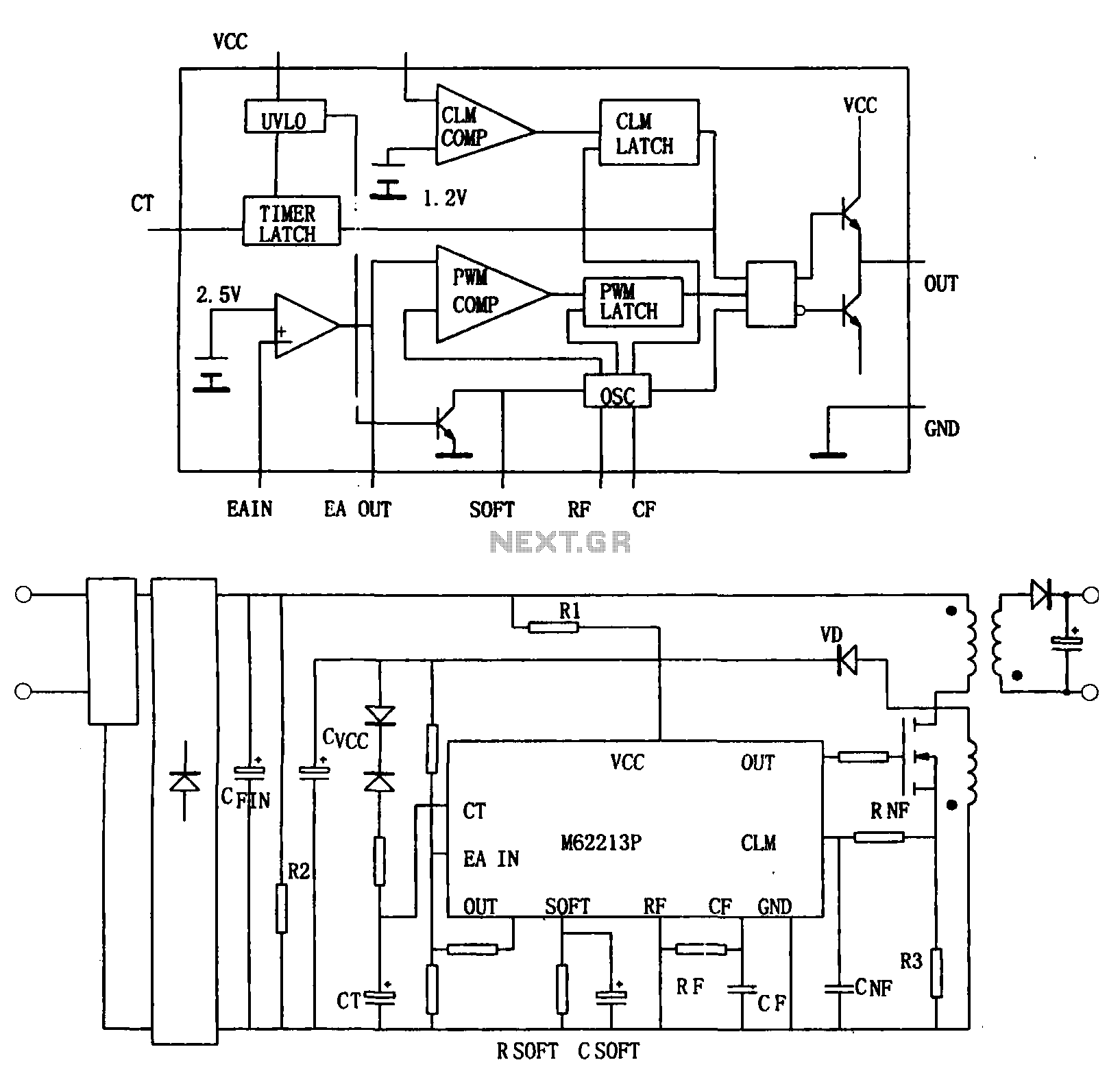
Figure (a) illustrates a block diagram of the internal architecture of the M62213FP, which is a high-speed switching power supply controller. This device includes an oscillator, PWM comparator, error amplifier, output circuit, over-voltage protection, timing latch circuit, over-current protection...
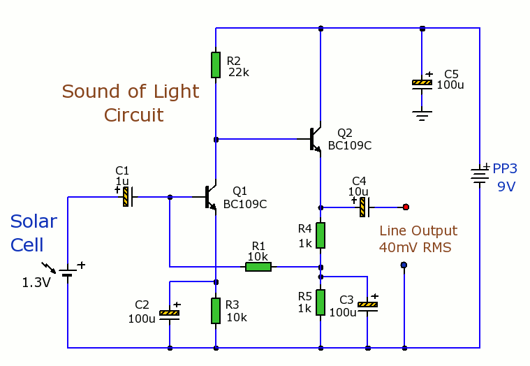
Solar Cells Light-Sound Converter. This is an experimental circuit that converts light into sound. The Solar Cells Light-Sound Converter is an innovative circuit designed to transduce light energy into acoustic signals. This experimental setup utilizes photovoltaic cells to capture ambient...
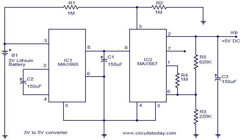
Voltage converter circuit diagram for converting 3 volts to 5 volts using CMOS monolithic ICs MAX660 and MAX667, which functions as a positive voltage regulator. The voltage converter circuit utilizes the MAX660 and MAX667 integrated circuits to step up a...
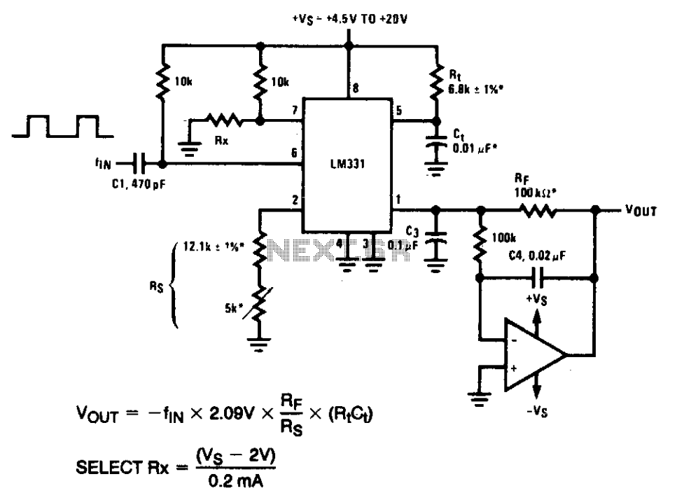
In the precision circuit, an operational amplifier provides a buffered output and also functions as a 2-pole filter. The ripple will be less than 5 mV peak for all frequencies above 1 kHz, and the response time will be...

This design circuit serves as a converter utilizing the LM2623A ratio adaptive circuit to drive a digital camera motor. It generates 5 volts from input voltages that range between 1.8 and 4.5 volts. The circuit's duty cycle, while not...
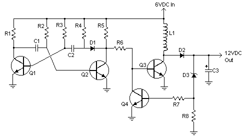
This inverter circuit can provide up to 800mA of 12V power from a 6V supply. For example, you could run 12V car accessories in a 6V car. The circuit is simple, about 75% efficient and quite useful. By changing...