
Delayed Alarm Circuit
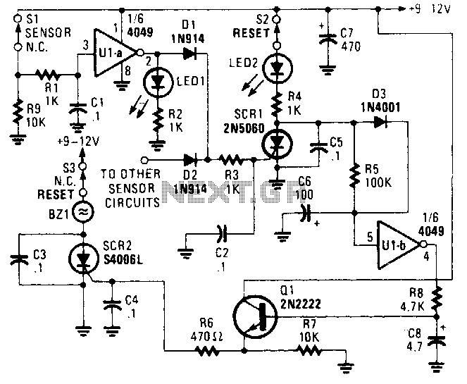
This low output is applied to the base of transistor Q1, keeping it off. Without a trigger voltage at the gate of SCR2 (through Q1), SCR2 remains off, and buzzer BZ1 does not activate. If switch SI opens, the input of U1-a is pulled low through R9, causing U1-a's output to go high and illuminating LED1. This high signal is also sent to the gate of SCR1 via diode D1 and resistor R3, turning SCR1 on. With SCR1 conducting, the charge on capacitor C0 discharges, pulling the input of U1-b at pin 5 low and forcing its output high. Capacitor C8 begins to charge through resistor R8 to a voltage slightly below the positive supply voltage. Transistor Q1 remains off until C8 reaches a voltage sufficient to turn Q1 on, providing enough time to enter the protected area and disable the alarm before it sounds. Once C8 reaches the necessary charge, Q1 activates and supplies gate current to SCR2 through resistor R6, turning on SCR2 and triggering BZ1. If the circuit is reset prior to the expiration of the delay, no alarm will sound. The delay duration can be adjusted by changing the values of either or both C6 and R5; increasing their values will lengthen the delay, while decreasing them will shorten it. All switches in the circuit are of the normally-closed (NC) type. Switch SI can be any NC security switch, while switch S2 may be a pushbutton or toggle switch. Switch S3 is designated solely for disabling the buzzer (BZ1) and can be any type, from a key-operated security switch to a concealed toggle switch.
The alarm/sensor circuit operates effectively by utilizing a combination of SCRs and transistors to create a reliable detection and delay mechanism. The inclusion of the 4049 hex inverter allows for signal inversion, which is crucial in maintaining the state of the alarm system during the initial power-up phase. The design ensures that the system remains inactive as long as the protected area is secure, providing a grace period for authorized entry.
The feedback loop established through the SCRs and the capacitors allows for a smooth transition from a non-alarmed state to an alarmed state, minimizing false alarms while ensuring prompt activation when required. The use of discrete components such as resistors, capacitors, and diodes allows for fine-tuning of the circuit's response times, providing versatility in various applications.
Moreover, the selection of normally-closed switches enhances security measures, as any unauthorized opening will trigger the alarm system. This design is particularly suitable for security applications where immediate notification of breaches is critical. The circuit can be adapted for different environments by adjusting component values and switch types, making it a flexible solution for various security needs. Overall, the alarm/sensor circuit presents a robust design that effectively balances sensitivity and delay, ensuring optimal performance in securing protected areas. The alarm/sensor circuit shown is built around two SCRs, a transistor, a 4049 hex inverter, and a few support components, all of which combine to form a closed-loop detection circuit with a delay feature. The delay feature allows you to enter a protected area and deactivate the circuit before the sounder goes off.Assuming that the protected area has not been breached (i.e., SI is in its normally-closed position), when power is first applied to the circuit, -a positive voltage is applied to the input of Ul-a through SI and R1, causing its output to go low.
That low is applied to the gate of SCR1, causing it to remain off. At the same time, C6 rapidly charges toward the supply rail through S2, LED2, R4, and D3. The charge on C6 pulls pin 5 of Ul-b high, causing its output at pin 4 to be low. That low is applied to the base of Ql, keeping it off. Because no trigger voltage is applied to the gate of SCR2 (via Ql), the SCR remains off and BZ1 does not sound.But should SI open, the input of Ul-a is pulled low via R9, forcing the output of Ul-a high, lighting LED1. That high is also.applied to the gate of SCR1 through D1 and R3, causing SCR1 to turn on. With SCR1 conducting, the charge on Co decays, the input of Ul-b at pin 5 is pulled low, forcing its output high, slowing charging C8 through R8 to a voltage slightly less than the positive supply rail.
Transistor Ql remains off until C8 has charged to a level sufficient to bias Ql on, allowing sufficient time to enter the protected area and disable the alarm before it sounds. Once C8 has developed a sufficient charge, Ql turns on and supplies gate current to SCR2 through R6, causing the SCR to turn on and activate BZ1.
If the circuit is reset before the delay has timed out, no alarm will sound. The delay time can be lengthened by increasing the value of either or both C6 and R5; decreasing the value of either or both of those components will shorten the delay time. All of the switches used in the circuit are of the normally-closed (NC) variety. Switch SI can be any type of NC security switch. Switch S2 can be either a pushbutton or toggle switch. Because S3 is used to disable the sounder (BZ1) only, anything from a key-operated security switch to a hidden toggle switch can be used.
🔗 External reference
Related Circuits
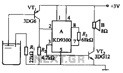
Changing the values of Ri, R2, Cl, and C3 can modify the alarm tone. The circuit utilizes KD9300 music integrated circuits. The circuit described is designed to generate an alarm tone through the manipulation of specific component values within the...
The SN754410 Dual Motor Control circuit is illustrated below. It is straightforward in design, with the PIC serving as the central processor. The main components included in the schematic are the 7805 voltage regulator, the 18F452 microcontroller, and the...
This circuit generates dual-tone bell sounds similar to those found in standard doorbell units. It is applicable in various contexts beyond doorbells. The circuit, as depicted in the diagram, produces a "Ding-tone" when switch P1 is pressed and a...
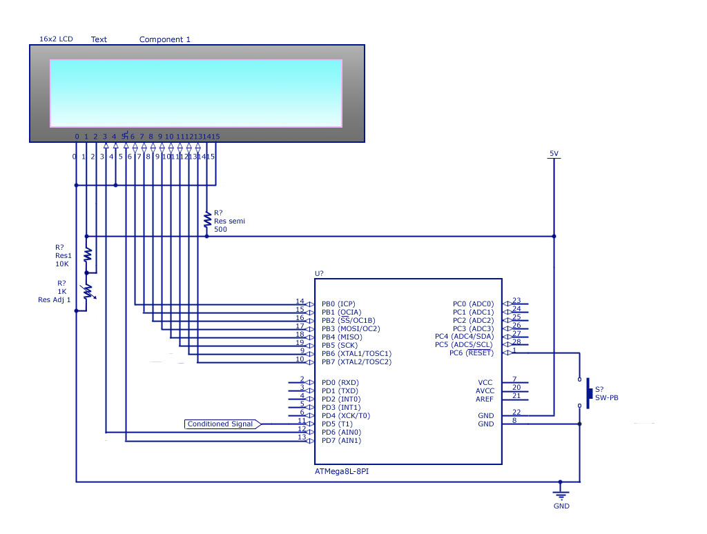
A simple frequency meter or frequency counter circuit featuring an LCD display and an AVR microcontroller. This includes a DIY schematic circuit diagram and embedded C code. The frequency meter circuit is designed to measure the frequency of input signals...
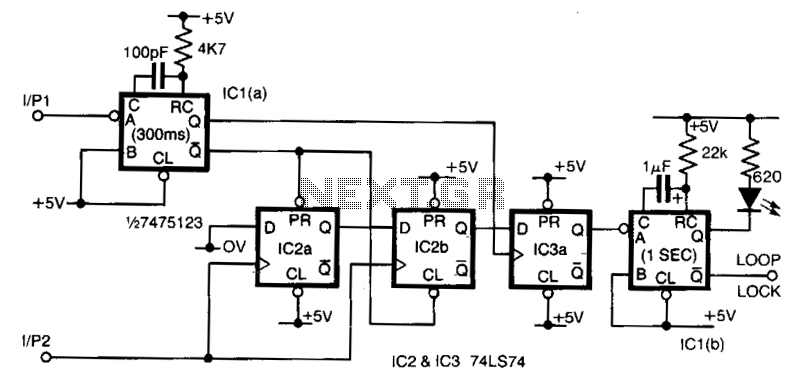
Input 1 functions as a gating period, during which a single rising edge on input 2 produces a logic 1 output. Any other input that indicates non-identical frequencies results in a logic 0 output. IC1a converts input 1 into...
A circuit that activates a relay upon detecting audio pulses from one channel of an MP3 player. The intention is to synchronize recorded audio pulses with music to control a motor for mouth movement. For a stereo player, music...
Warning: include(partials/cookie-banner.php): Failed to open stream: Permission denied in /var/www/html/nextgr/view-circuit.php on line 713
Warning: include(): Failed opening 'partials/cookie-banner.php' for inclusion (include_path='.:/usr/share/php') in /var/www/html/nextgr/view-circuit.php on line 713