
Differential A/D Converter circuit CA3110
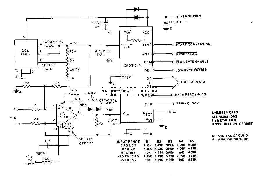
The BiMOS CA3140 operational amplifier is a versatile component characterized by its high bandwidth and rapid response to signal changes. This op amp is particularly effective in applications requiring precise signal conditioning and amplification. Its ability to function near the negative supply rail enhances its utility in various circuit designs, allowing for greater flexibility in system configurations.
In scenarios where the input voltage may exceed the supply voltage VDD, it is crucial to protect the op amp from potential damage caused by overvoltage conditions. The implementation of a clamp diode serves as an effective protective measure. By connecting a diode from pin 8 of the CA3140 to the VDD supply, any excess voltage can be safely redirected, preventing the op amp from being subjected to harmful levels.
The schematic for this configuration should include the CA3140 op amp, clearly labeling the input and output terminals, as well as the power supply connections. The clamp diode should be represented with its anode connected to pin 8 and the cathode connected to the VDD. This arrangement ensures that the op amp operates within its specified voltage limits, thereby enhancing reliability and performance in high-frequency applications. Proper grounding and decoupling capacitors should also be included in the design to minimize noise and improve stability.By using an op amp BiMOS CA3140 provides good orientation skills for high bandwidth signal input, and can quickly adjust the energy output at its terminal CA33IO WINE. The CA3140 can also lead to near the negative supply rail. If the sequencing system power or voltage input is known to cause the op amp to drive above the supply VDD, a clamp diode can be added from pin 8 of op amp to power supply VDD. 🔗 External reference
Related Circuits
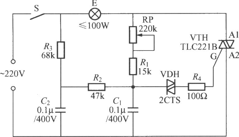
To address the lag and light transition issues, a Triac dimming light circuit featuring a dual time constant can be employed. This circuit enhances the resistor-capacitor network formed by R3 and C2. The reduced charge on capacitor C1 can...
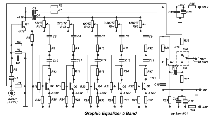
Another unit of graphic equalizer with five bands. The primary distinction from other circuits is the use of transistors instead of integrated circuits (ICs), and the power supply operates at +/- 24V DC, which ensures low distortion and greater...
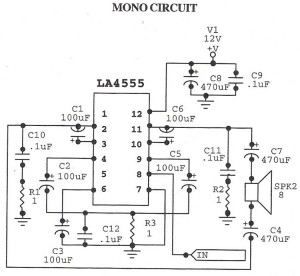
The following circuit illustrates an audio amplifier mono circuit diagram. This circuit is based on the LA4555 integrated circuit (IC). Features include a mono configuration and a power output of 2.3 watts. The audio amplifier circuit utilizing the LA4555 IC...
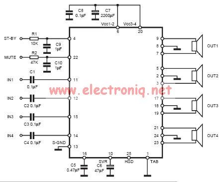
The input capacitor is used for low-frequency cut-off, with a standard value of 0.1 µF, resulting in a cut-off frequency of approximately 16 Hz. The input capacitor plays a critical role in electronic circuits, particularly in signal processing and audio...
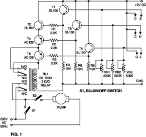
This simple water detector circuit utilizes alternating voltage to prevent the corrosion of the electrodes. It is straightforward to construct and employs N1 as a trigger Schmitt gate that generates the AC signal. When an electrical conductor, such as...
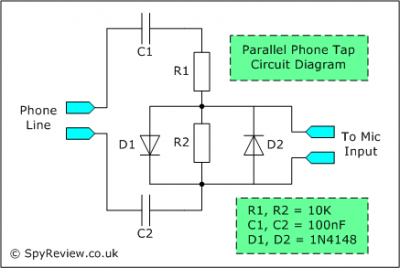
This file contains a schematic for a simple wiretap and instructions for connecting a small tape recorder control relay to the phone line. The discussion begins with an overview of various types of taps, including transmitters, wired taps, and...
Warning: include(partials/cookie-banner.php): Failed to open stream: Permission denied in /var/www/html/nextgr/view-circuit.php on line 713
Warning: include(): Failed opening 'partials/cookie-banner.php' for inclusion (include_path='.:/usr/share/php') in /var/www/html/nextgr/view-circuit.php on line 713