
Differential amplifier circuit

The differential amplifier is a critical component in analog signal processing, widely used for its ability to amplify the difference between two input signals while rejecting common-mode noise. The configuration begins with two matched transistors, VT1 and VT2, which are essential for maintaining balance and ensuring that both transistors operate under similar conditions. This matching is crucial for minimizing thermal drift and ensuring consistent performance across varying temperatures.
In the first configuration, when switch K is in the O position, the circuit is set up to operate as a standard differential amplifier. The quiescent point, or the DC operating point, is adjusted using the potentiometer RP, allowing for fine-tuning of the amplifier's response to input signals. The absence of negative feedback in the differential mode preserves the amplifier's gain characteristics, thus providing a high degree of sensitivity to differential signals. The shared emitter resistor (RE) plays a vital role in stabilizing the common-mode gain, which is critical in applications where noise rejection is paramount.
In the second configuration, with switch K in the alternate position, the circuit transforms into a constant current source. This is achieved by utilizing transistor VT3, which replaces the emitter resistor RE. By implementing a constant current source, the circuit gains improved performance in suppressing common-mode signals, which can be particularly beneficial in environments with significant electromagnetic interference. This enhancement is due to the constant current source providing a stable biasing condition, which minimizes variations in the output due to fluctuations in the supply voltage or temperature changes.
Overall, the design of this differential amplifier circuit emphasizes stability, precision, and the ability to effectively suppress unwanted noise, making it suitable for various applications in instrumentation, audio processing, and communication systems.Differential amplifier stability, zero drift suppression, is a common amplifier. Differential amplifier circuit shown in Figure, by two parameters identical transistors VT1, VT 2 (both 3DG6) components. Component parameter reference value as shown in FIG. Both circuits form is as follows: 1) When the switch K is connected when O end, put up a typical differential amplifier. Decay is used to adjust the potentiometer RP VT1, VT2 quiescent operating point, so that the input signal Ui o, double-ended output voltage Ue O.
RE for the two shared emitter resistor, its differential mode signal number no negative feedback effect, and thus does not affect the differential mode voltage gain, but for the common-mode signal has a strong negative feedback effect can be effectively suppressed zero drift system stable amplifier quiescent point. 2) When the switch K is connected end when constituting a constant current source of the differential amplifier.
A constant current source transistor VT3 employed to replace fat emitter resistance RE, the differential amplifier can be further improved co-suppression capability mode signal.
Related Circuits
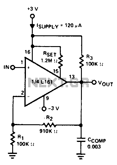
The amplifier is 3 dB down at 100 kHz and has a slew rate of 0.02 V/µs. The amplifier's performance characteristics indicate that it experiences a 3 dB attenuation at a frequency of 100 kHz. This specification suggests that at...
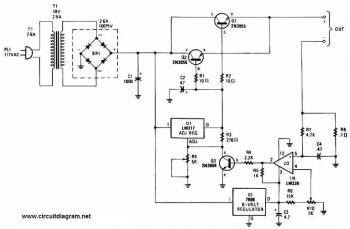
This battery charger circuit is regulated and adjustable, enabling it to charge most NiCAD batteries. It can accommodate both single cells and multiple battery cells connected in series or parallel. The maximum voltage of the batteries should not exceed...
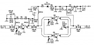
This RF amplifier circuit delivers a power output of 4 Watts at a frequency of 900 MHz. It utilizes Wilkinson power dividers in the base and collector circuits of transistors Q2 and Q3. Two SD1853 driver application transistors are...
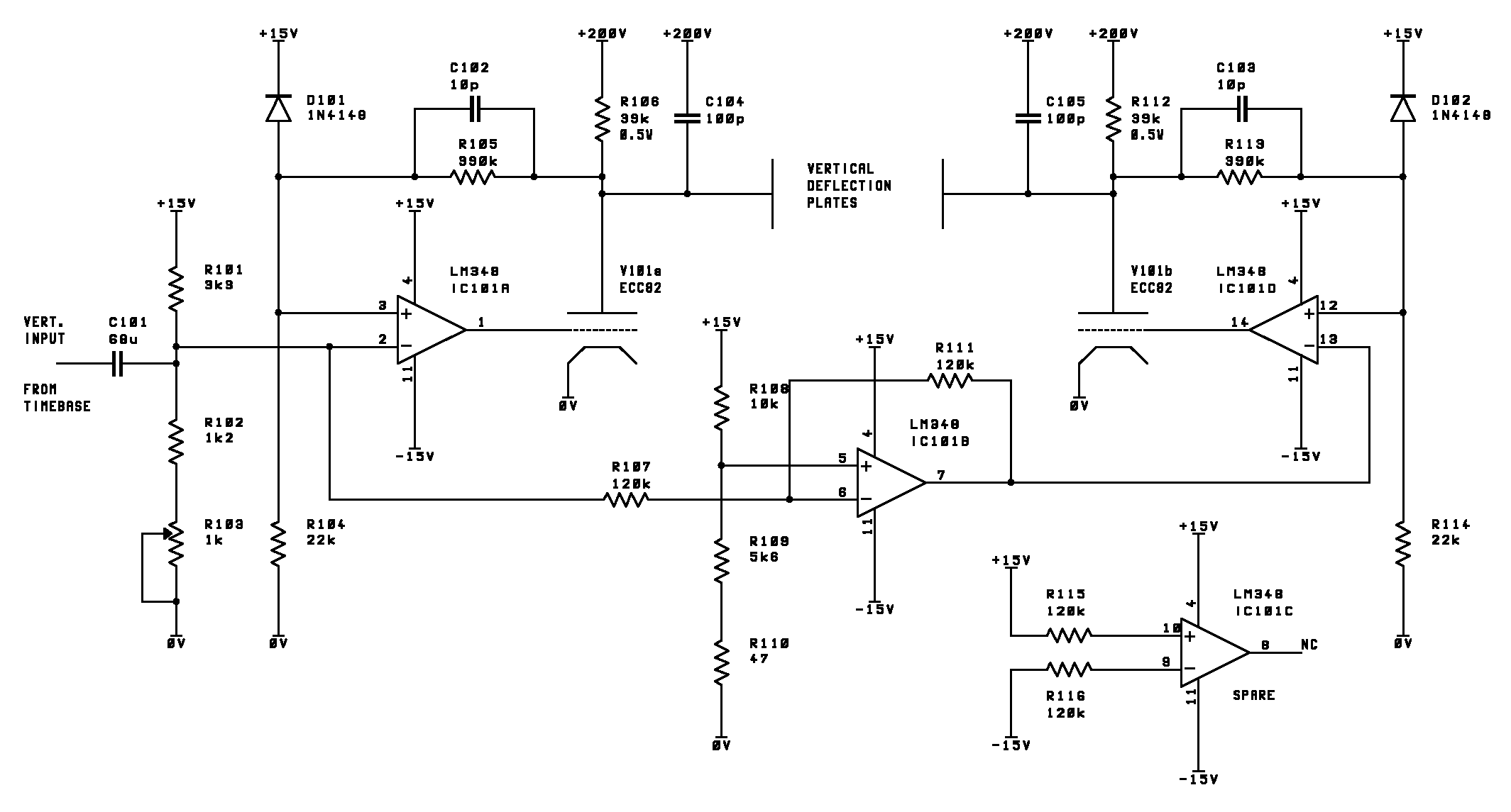
This page outlines the development of electronics for displaying a monochrome video image on an electrostatic oscilloscope tube. This work complements the Electron Optics section in the Experiments category. The primary objective is to showcase a moving video image...
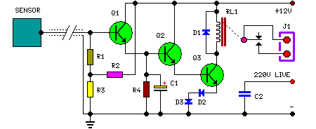
The purpose of this circuit is to animate shop windows using a capacitive sensor positioned behind a postcard-like banner. The card is placed against the glass inside the shop window, allowing visitors to activate the relay by placing their...
This simple and inexpensive audio amplifier can be constructed using a couple of TO-220 monolithic Darlington transistors for the push-pull output stage. The frequency response is flat within 1 dB from 30 Hz to 200 kHz, with typical harmonic...