
Digital delay circuit lamp circuit 2
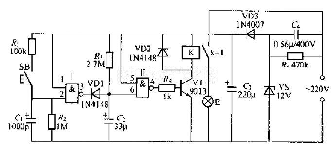
The digital delay lamp circuit is designed to provide a controlled delay in the operation of a lamp using a 2-input NAND gate integrated circuit. The circuit begins with a capacitive voltage rectifier that ensures a stable DC voltage supply. The two NAND gates are configured such that the output responds to changes in the input states, specifically focusing on the transition from low to high.
Upon energization, the initial state of the NAND gates is crucial. Both inputs are typically held at a high logic level (1), which keeps the output of one gate in a low state (0). This is due to the steady state conditions of the circuit, where the charging of capacitors influences the logic levels. When an external switch (SB) is pressed, the first input transitions from low to high, triggering a change in the output state. The output of the first gate switches to low, allowing current to flow through diode VD1, which then influences the second input of the second NAND gate.
As the second input also goes low, the output of the second NAND gate transitions to high, energizing the relay (K) that powers the lamp (E). This relay operation is critical as it provides a physical connection to the lamp, allowing it to illuminate. The design includes a timing element, where after the button is released, the output remains high for a period determined by the RC time constant of the charging circuit. The time constant is influenced by the values of the resistors and capacitors used in the circuit.
After approximately 40 seconds, the charge on the capacitor reaches a level that causes the output to lose its low state, deactivating the relay and turning off the lamp. The circuit design emphasizes the importance of grounding the input sides of the NAND gates to prevent interference, ensuring reliable operation. The use of high-quality components, such as CBB polypropylene capacitors rated at 100V, and the selection of a suitable electromagnetic relay rated for DC12V, are essential for the longevity and performance of the circuit. Overall, this digital delay lamp circuit effectively demonstrates the application of logic gates in practical electronic designs, providing both functionality and a delay mechanism for controlling lighting.A 2-input NAND gate integrated circuit fabrication of digital delay lamp circuit, VD3, vs, after Composed of simple capacitive voltage rectifier buck crossing the half line, th e circuit is energized, C. A terminal is output ipv about the stability of the entire controller DC voltage power supply. Figure, the door I the door O feet and the feet of are usually island level 1, so that both open state, while the other gate II input That is due to the end of foot in steady state C: it has charged the wires, so it is high level 1 so the door. II output terminal pin low level state, the diode VT end, the relay K little trick. E lamp does not light when pressed SB, by R. power to (j g of electricity, so that the door I input feet from the original low-to-high level 1 state, the output goes low O state, diode VDI conduction, such as on the adoption of VDI discharge.
therefore, another rjU the one input terminal feet becomes a low level. state, the output terminal pin goes high l state, high hills l level NIE Yi Rt make wr conduction, the relay K is energized, its power make contact k1 is closed, the lamp is powered hair E dagger when released SB, f1 T and the output goes high l, VD1 off, f. but also by R. charging about after 40s time (depends on R, and (1, wide electrical time constant), f. F level rose to a certain value, the door lose meaning. low., VT end, K release, lamp E goes out. door 1, f] [I can CD1011 digital integrated circuits inside two intact and two NAND gates brother does not use NAND gates should the grounding of all its input side, to eliminate possible interference caused .c.
requires the use of CBB, lOOV polypropylene capacitors and other type K with JZC-22F, DC12V power in a small electromagnetic relay.
Related Circuits

The LM1875 is a monolithic audio amplifier that provides very low distortion and high-quality performance for audio amplifier projects. The LM1875 delivers 20 watts into loads of 4 Ohms or 8 Ohms. The LM1875 audio amplifier is designed for applications...
Driving a series of white LEDs allows for a consistent current to flow through each LED, resulting in uniform brightness. However, a disadvantage of this series configuration is that the driving voltage must account for the forward voltage drop...
In the wiper-delay schematic presented, when the ignition is activated, Di maintains a regulated +12 V DC. Upon closing SI, CI bypasses transients and allows this +12 V DC to reach the resistor divider R2-R3, generating a TTL high...
This capacitance meter circuit is similar to previous meter circuits, but it utilizes transistors instead of logic gates. A schematic diagram is provided. The capacitance meter circuit operates by measuring the capacitance of a capacitor through a time-based method. The...
This circuit is an RMS-calibrated AC voltmeter that provides average readings. Removing capacitor C2 eliminates the averaging function, resulting in a precision full-wave rectifier, while removing capacitor C1 transforms the circuit into an absolute value generator. The operation of...

A capacitor step-down DC power supply circuit is presented. This circuit eliminates the need for power transformers, utilizing capacitive voltage drop rectification and regulation, which significantly reduces the overall size of the circuit. The circuit includes a capacitor step-down...