
Solid-State Windshield-Wiper Delay
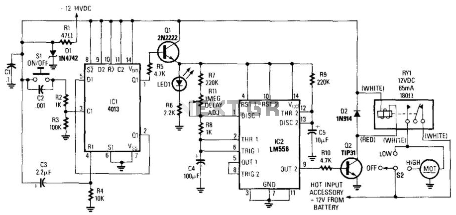
The wiper-delay circuit is designed to provide a timed operation of windshield wipers based on the ignition state and user input. The 4013 CMOS flip-flop (IC1) is crucial for maintaining the state of the wiper control signal, ensuring that the wipers only operate when intended. The resistor divider R2-R3 is essential for generating the TTL signal required to trigger the flip-flop, while the filtering components (R4 and C3) protect against false triggering due to electrical noise.
The astable configuration of IC2 generates a square wave output that determines the timing for the wiper operation, with the resistors R7, R8, and R11 setting the frequency and thus the delay between wiper cycles. The monostable section, controlled by R9 and C5, ensures that each wiper activation lasts for a predetermined duration, allowing for effective clearing of the windshield. The interaction between Q1 and IC2 is particularly noteworthy, as it modifies the expected timing characteristics due to the active current sourcing from Q1, leading to faster charge and discharge cycles for C4.
The inclusion of Q2 and RY1 allows for the actual control of the wiper motor or mechanism, with D2 providing protection against voltage spikes that could occur when the relay is turned off, thereby ensuring the longevity and reliability of the circuit. Overall, this schematic represents a robust solution for controlling windshield wipers with adjustable timing features, enhancing driver convenience and safety. In the wiper-delay schematic shown, with the ignition on, Dl maintains regulated +12 Vdc. When SI closes , CI bypasses transients and passes this +12 Vdc to divider R2-R3, producing a TTL high at pin 3 of IC1, a 4013 CMOS dual leading-edge triggered D-type flip-flop. Filter R4/C3 keeps IC1 from triggering erroneously when the ignition is on. When SI is pressed, output Ql (pin 1) of IC1 latches high, turning on Ql, which conducts via R5, turning on IC2; LED1 indicates power, and R6 sets the current.
Because IC2 depends on Ql for power, IC2 stays off until Ql turns on. The left half of IC2 is an astable, with its delay set by R7, R8, Rll, and C4. The right half of IC2 is a monostable, with its pulse duration set by R9 and C5. With the values used, you might expect Rll to vary the delay from about 15 to 84 seconds, with a 2.42-second monostable pulse operating the wiper blades on each cycle. However, the actual delay will range between 2 to 18 s, with a 1-s monostable pulse on each cycle. That discrepancy stems from the fact that IC2 is being fed from the emitter of Ql, rather than directly from the regulated +12-V supply.
Transistor Ql acts as an active current source, charges and discharges C4 faster than it ordinarily would. The astable output (OUTi, pin 5) is tied to TRIG2 (pin 8). When OUT2 (pin 9) becomes high, Q2 is biased via RIO and current flows through RY1, with D2 dissipating back-emf when RY1 shuts off.
🔗 External reference
Related Circuits
The circuit is designed for sound and light control of stairway and walkway lighting. It features high immunity and includes soft-start and over-current protection mechanisms. During the day, the photosensitive resistor has low resistance, resulting in a low voltage...

Long delay times can be derived from a 555 timer with reasonably sized capacitors if an integrator circuit is used. The capacitor's charging time with an integrator circuit can be much longer than with a conventional 555-timer configuration. The 555...
This circuit is a robust light control delay switch with strong anti-interference capabilities. It requires a specific sequence of claps to activate the lamp, which will illuminate for a predetermined duration before automatically turning off. The circuit design is...
This switch allows the model train at such a station to automatically slow down. The train stands for a certain amount of time and then slowly pulls back. You do not need to stop the train. The relatively simple...
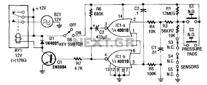
In this circuit, IC1A and IC1B serve as a monostable multivibrator. Any input from the sensors SI through S5 triggers IC1A to produce a logic low signal, which activates IC1B, turning on Q1 until the capacitor C3 discharges through...
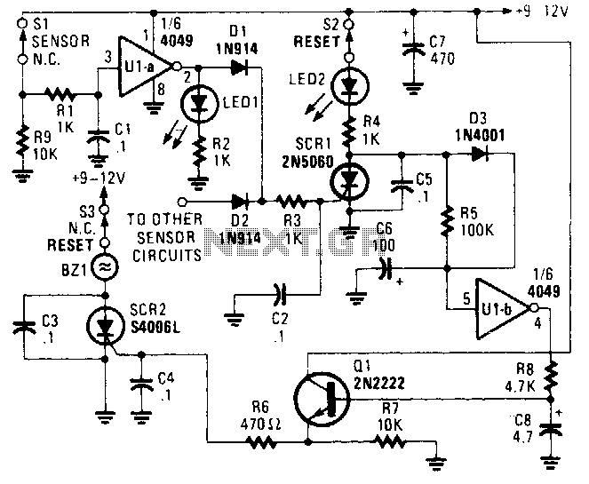
The alarm/sensor circuit is constructed using two SCRs, a transistor, a 4049 hex inverter, and several supporting components, which together create a closed-loop detection circuit featuring a delay mechanism. This delay allows entry into a protected area and deactivation...