
FET Voltage Regulator
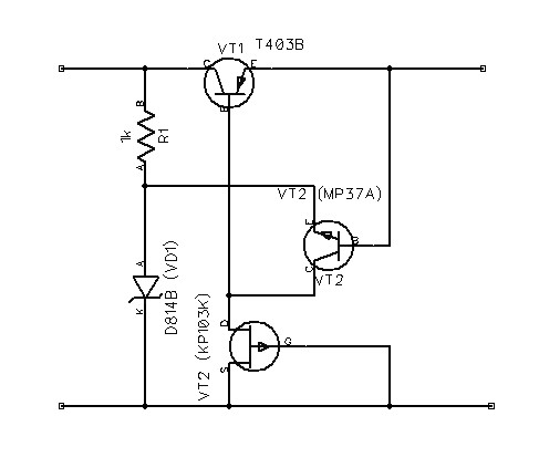
The voltage regulator circuit described is an essential component in various electronic applications, providing stable output voltage and current. The use of a Field Effect Transistor (FET) in the feedback loop allows for efficient voltage regulation, responding dynamically to changes in input voltage. The FET VT3 plays a critical role in maintaining the stability of the output voltage by adjusting the load conditions on transistor VT2, which enhances the overall performance of the regulator.
The 2N3055 power transistors are well-known for their ability to handle high currents, making them suitable for applications requiring significant power. The configuration of four 2N3055 transistors in parallel increases the current handling capacity, allowing the regulator to supply up to 10A at 13.8V. The LM109 regulator IC provides a reliable reference voltage and control mechanism, ensuring that the output remains stable under varying load conditions.
The circuit's design incorporates a diode bridge rectifier, which converts the AC input voltage into a DC output. This rectification process is crucial for the operation of the regulator, as it allows for the smooth delivery of power to the load. The adjustable output voltage feature adds versatility, enabling the circuit to be tailored to specific application requirements.
Overall, this voltage regulator circuit is a robust solution for powering devices that require a stable voltage supply, making it a valuable design in the field of electronics.The schematic diagram come from circuit: The Voltage Regulator With a Field Effect Transistor power supply. Go to that page to read the explanation about above power supply related circuit diagram. Feature of this transistor compensation voltage (see picture) - used in the feedback field effect transistor VT3, which acts as a dynamic load for the
transistor VT2. Because of this factor increases the voltage regulation: when the input voltage from. This regulator power supply schematic diagram is the same as the previous 5V 10A regulator circuit with a little modification and have the ability to supply less current up to 3 amperes at voltage of 5V. The circuit is built. This is a dc regulator circuit which will give output voltage of 13. 8V with current output about 10A. The circuit use 4 pieces of power transistor 2N3055 to boost the electric current, to make the circuit capable to deliver 10A.
This power supply regulator circuit can provide current up to 10 amperes at a voltage 5 V. The circuit is built from a complete 5V regulator IC LM 109 series from National Semiconductor. While for the current amplifier assisted by. To supply the high voltage converter suitable source of alternating voltage 12 V / 800 mA. An alternating voltage is rectified by a diode bridge with an allowable current of 1 A. Converter output voltage is adjustable between 0. . We aim to transmit more information by carrying articles. Please send us an E-mail to wanghuali@hqew. net within 15 days if we are involved in the problems of article content, copyright or other problems. We will delete it soon. 🔗 External reference
Related Circuits
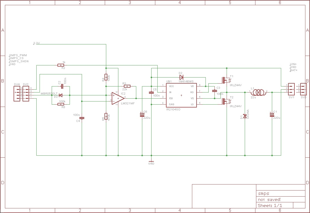
The circuit receives an input voltage (Vin), which is processed through a Switch Mode Power Supply (SMPS) utilizing two MOSFETs driven by an IR2104 driver. The output is directed to the battery positive terminal (Bat+). An LM321 operates as...
If the offset value exceeds 5mV, adjust this value by experimenting with resistors, starting with 220K, connected from test point Z (the junction of R22 and R23) to +V if there is a negative voltage, or to -V if...

When the supply voltage drops below a minimum threshold, it is often advisable to disconnect the supply from the system to prevent poor performance or erratic operation. The circuit presented achieves this with minimal cost, board space, and complexity....
This application note outlines the implementation of a PSoC (Programmable System-on-Chip) device for controlling a Brushless DC (BLDC) windscreen wiper motor in automotive applications. The design incorporates LIN Bus 2.0 to facilitate the control of wiper operations. The document...
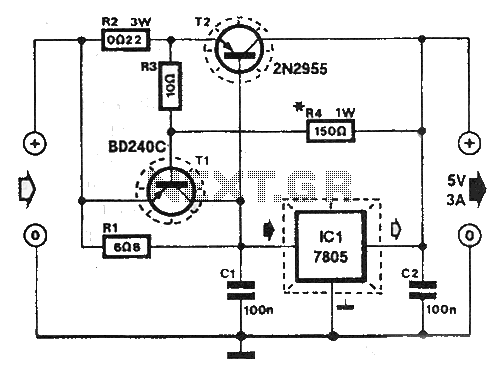
At this voltage regulator prototype the maximum current, with output shortcircuited it was only 0.5 A, so no overheating occurred. In this DC voltage regulator circuit, T1 is for current limitation. As soon as the voltage on the R2...
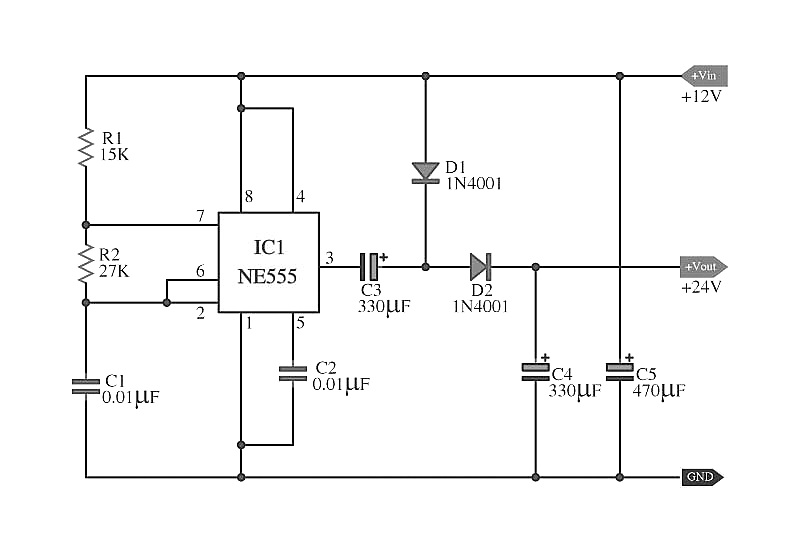
The capacitors C5 work in conjunction with IC1, while the resistors R1 and R2, along with capacitors C1, form an astable multivibrator square wave generator. This generator outputs a frequency of approximately 2 kHz from pin 3 of IC1....