
Dual adjustable power supply circuit
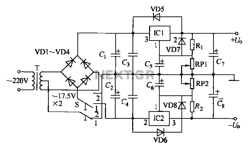
This circuit design offers a versatile solution for adjustable voltage regulation in various electronic applications. The use of the LM317 and LM337 regulators allows for both positive and negative voltage outputs, making it suitable for dual power supply requirements. The adjustable potentiometers (RP1 and RP2) enable fine-tuning of the output voltage, which is critical for applications requiring precise voltage levels.
The transformer steps down the AC voltage from the mains to a lower AC voltage, which is then rectified by the bridge rectifier into a DC voltage. The filtering capacitors (C1 and C2) smooth out the rectified voltage, providing a stable input to the voltage regulators. The inclusion of sampling resistors (Ri) ensures that the feedback loop for the voltage regulators operates correctly, maintaining the desired output voltage.
In applications where the circuit is configured for single output mode (using S2), the circuit effectively doubles the output voltage range, providing flexibility for various load requirements. The diode configuration (VD1 to VD4) protects the circuit from reverse polarity and voltage spikes, ensuring reliability and longevity of the components.
The choice of components, such as the 1N4001 diodes, is appropriate for the current levels typically expected in such circuits, while the selected capacitors are rated for high voltage to prevent breakdown under operating conditions. Additionally, the thermal management considerations, such as the use of heat sinks, are crucial for maintaining the performance and safety of the voltage regulators, especially under higher load conditions.
Overall, this circuit is well-suited for applications that require adjustable voltage levels, such as power supplies for testing equipment, audio amplifiers, and other electronic devices needing custom voltage inputs. Circuit principle: This circuit uses three-terminal adjustable integrated voltage regulator, S gear set, the power supply voltage via a step-down transformer 17. 5VX2 alternati ng current voltage after the bridge rectifier, respectively, to give as gifts IC1,1C2 input end, the sampling resistor Ri, horses and adjustment potentiometer RP1, RP2 control, obtained at the output 1. 25-15V continuously adjustable voltage disabilities. When S 2 is placed, the dual output power transformer T as a single group using, after the power supply voltage by the rectifier filter, only to send IC1, get +1.
25-30V single power output. Among them, the resistance Rl, Rz: 240CZ, potentiometer RP1, RP2: 4. 7kf2; capacitance CL, C: 3300FcF/150V, G, C: 0.33 uF/63V.C5, C: lOtlFl50V; diode VD1 ~ VD4: 1N4001, VD5 ~ VD6: 1N4001} three terminal manifold ICl: LM317. IC2: LM337; switch S: KNX (Z 2). The power supply to all the capacitors are selected voltage greater than 50v, the two three-terminal adjustable power regulator block is about 15W, pay attention to add enough radiator,
Related Circuits
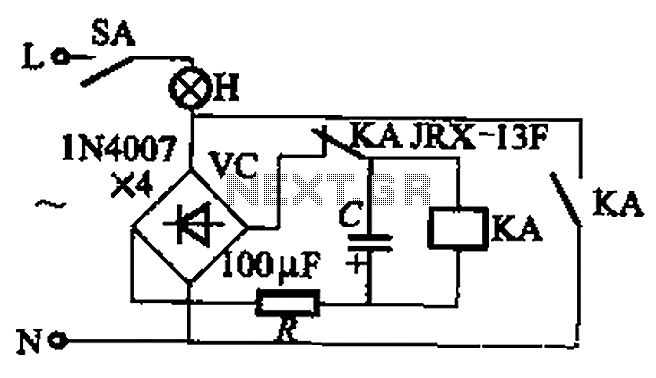
The circuit illustrated in Figure 13-3 consists of two configurations: (a) a DC power supply and (b) an AC power supply. Both configurations are utilized to control a relay. The flash frequency of the relay is determined by the...
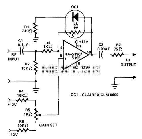
This circuit operates as a wideband adjustable automatic gain control (AGC) amplifier. It has an effective bandwidth of approximately 10 MHz and can handle RF input signal frequencies ranging from 3.2 to 10 MHz at levels between 40 mV...
This LED circuit replicates the initial LED sequence currently utilized by FISA for Formula One racing. It can also be employed with slot car sets, such as HO scale AFX, Life Like, or Tyco sets, or used in communication-controlled...
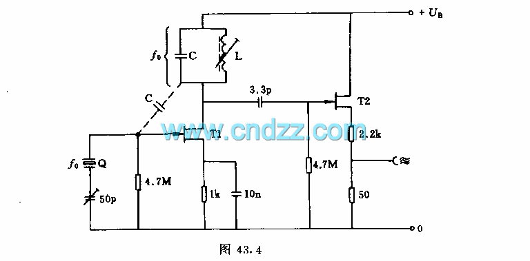
The oscillator employs a fundamental quartz crystal, capable of achieving an oscillation frequency of up to 10 MHz. The oscillator circuit is calibrated to the resonant frequency of the crystal. A capacitor, designated as C, with a value of...
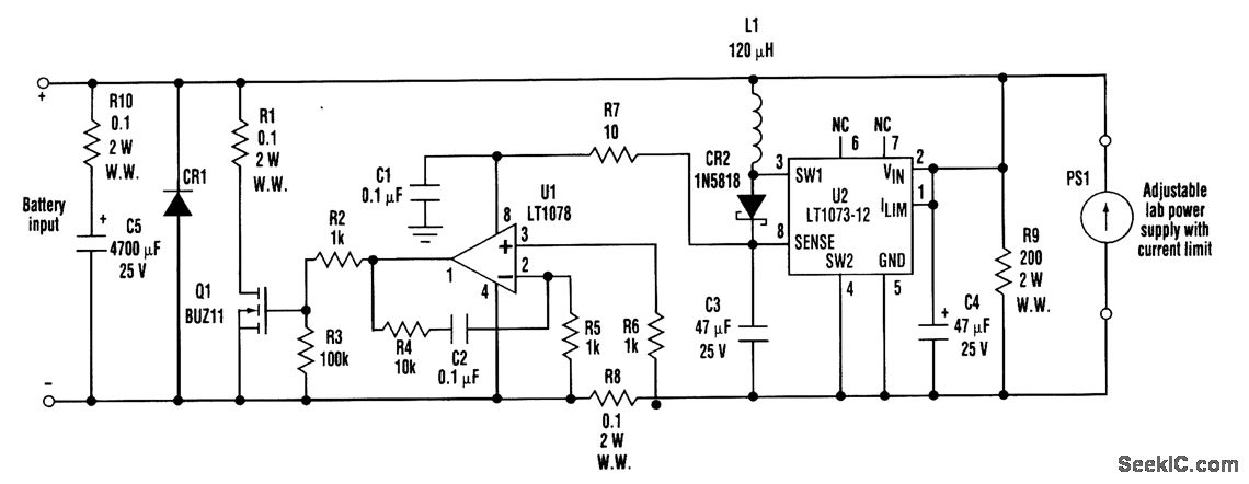
When developing a battery charger, using a real battery can be impractical. The battery simulator circuit described here serves as an alternative. The positive and negative terminals of the battery input should be connected in place of the actual...
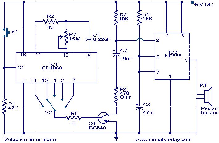
The following circuit illustrates a Selective Timer Alarm Circuit based on the 4060 Integrated Circuit (IC). Features include an automatic turn-off mechanism for the alarm after a specified duration. The Selective Timer Alarm Circuit utilizes the 4060 IC, which serves...