
Dual polarity single channel VCO

The circuit operates by utilizing a dual polarity input voltage, which allows for the modulation of an oscillating frequency based on the input signal. The first section involves the TL431, a programmable shunt voltage reference, which regulates the voltage to a stable 2.5V. This is achieved through the feedback mechanism set by the 1.2k ohm resistor, ensuring consistent output despite variations in load or input voltage.
The next part of the circuit incorporates the TLC272 operational amplifier, which is configured as a voltage buffer. This configuration is critical as it isolates the reference voltage from subsequent stages, preventing loading effects that could alter the voltage level. The output from the TLC272 at PIN7 serves as a crucial control voltage (VG) for further processing in the circuit.
The remaining sections of the schematic would typically include additional components such as oscillators or frequency control elements, which are influenced by the voltage derived from the TLC272. These components work in harmony to convert the stable reference voltage into a variable frequency output, enabling precise control over oscillation parameters based on the input voltage characteristics.
Overall, the schematic design reflects a well-structured approach to voltage regulation and frequency control, utilizing standard components to achieve reliable performance in electronic applications requiring dual polarity input processing.Schematic diagram for dual polarity single channel input voltage to oscillating frequency control. How circuit work! Circuit can be separated into 5 parts Reference voltage: TL431 and 1.2k resistor uses as 2.5V regulator. And IC TLC272 construct as voltage buffer circuit connect to the 2.5V also give 2.5V at PIN7 assign as (VG).
🔗 External reference
Related Circuits
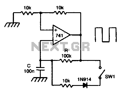
This circuit incorporates a Schmitt trigger and an integrator configured around a single operational amplifier (op-amp). The timing is regulated by an RC network. The voltage at the inverting input tracks the exponential charging of the capacitor within defined...
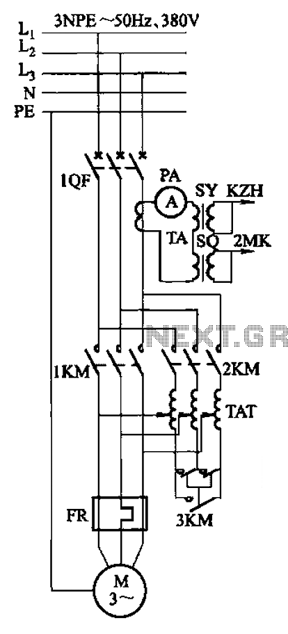
Autotransformer voltage starting, with an adjustable starting time of 30-60 seconds. It includes the SDJ electrode liquid level sensor of HJ-13 type, a pump control system box of HKD-21B type, 1MK level modules adopted by HKG-1SG type, 2MK start...
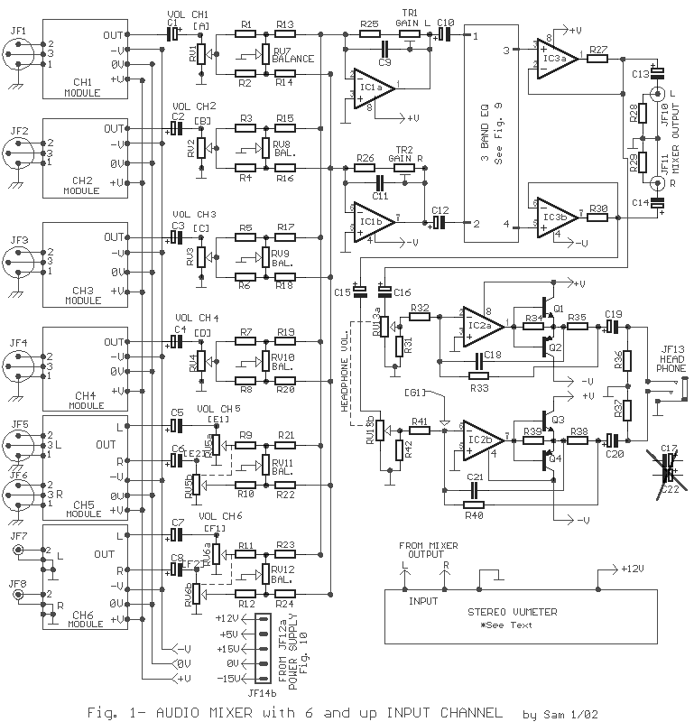
The main circuit of the 6-channel mixer consists of six input channels. Channels 1-4 are mono, while channels 5-6 are designed for music use. The number of input channels can be increased as desired. The output of each channel...
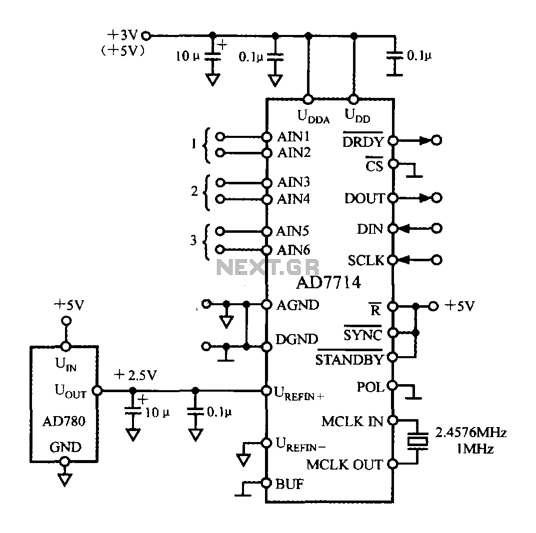
The typical application circuit for the AD7714 is illustrated in the accompanying figure. The UDD and UDDA terminals of the AD7714 can be connected to either a +3V or +5V power supply. The analog inputs are arranged as three...
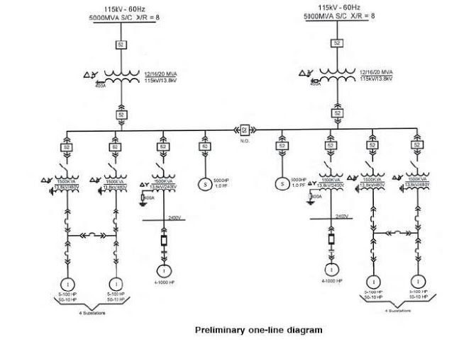
The single line diagram is a circuit diagram where a "one-line" representation illustrates the three phases of a three-phase power system. In addition to displaying the ratings and sizes of electrical equipment and circuit conductors, a well-drawn one-line diagram...
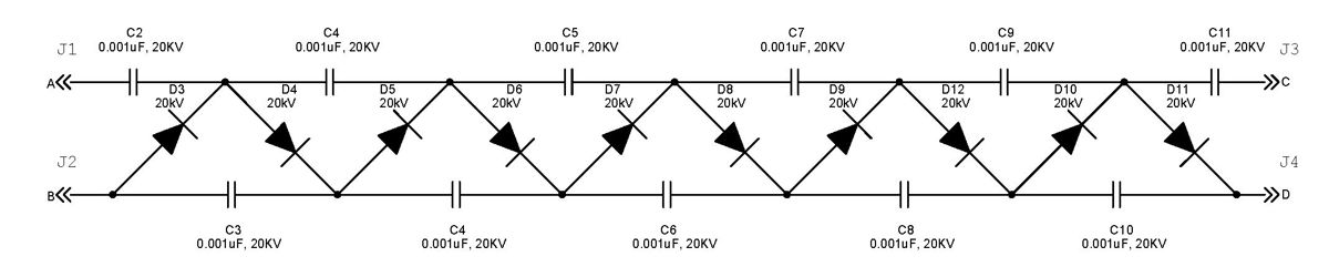
The Cockcroft-Walton multiplier employs a series of diodes and capacitors arranged in a cascade to generate a high-voltage DC potential from an AC input. This circuit topology utilizes diodes to charge capacitors in parallel and discharge them in series....