
Easy to adjust high-precision PWM pulse width modulation 12-bit DA converter
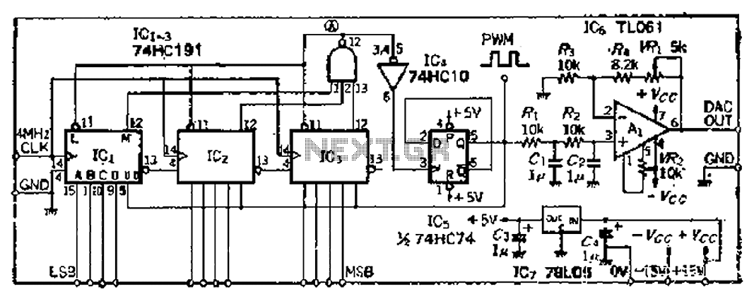
The described circuit functions as a pulse width modulation (PWM) generator and demodulator. The primary component, a series of integrated circuits (ICs), operates in two modes: counting up and counting down. Initially, the PWM clock signal is generated at a frequency that is 4096 times higher than the input frequency. This high-frequency signal allows for precise control over the output.
The counting mechanism is initiated by the ICi-IC3, which accumulates counts until a designated threshold is reached, at which point the output transitions to a maximum clock signal. This output is critical for maintaining synchronization with the input data. The voltage data is then loaded into IC3, while IC5 remains in a stable state, functioning as a bistable flip-flop that retains its state until prompted to change.
Once the maximum clock signal is achieved, the circuit transitions to a countdown phase. This phase continues until the minimum clock signal period is reached, indicating the end of the countdown. During this phase, the voltage signal facilitates the reloading of data into ICi-ICz, ensuring that the system can respond to new input signals efficiently.
The PWM demodulation process is integral to the operation of this circuit. The voltage data values are compared against the pulse count, allowing for accurate signal processing. The smoothing filter, composed of resistors R1 and R2 along with capacitors C1 and C2, plays a critical role in converting the PWM signal into a stable DC voltage. This conversion is essential for applications that require a steady voltage output.
Finally, the operational amplifier (OP) enhances the output signal by a factor of two, resulting in a voltage range from 0 to +10V. This amplification is particularly useful in applications where higher voltage levels are necessary for further processing or control tasks. Overall, the circuit is designed for robust performance in PWM applications, providing both high-frequency signal generation and accurate voltage regulation.4096 times the input frequency PWM clock signal, counts up (Q three ), until the base is full ICi-IC3 (sweet day), the output point d a MAX clock signal, which on the one hand the voltage data loaded into IClr rIC3, leaving the other dare steady Ics flip, Q ugly, namely, the number is in the state count down, and then began to count down until the point a fork outputs a MIN the clock signal period, the signal voltage on the one hand the data reloaded ICi ~ ICz, on the one hand to the bistable flip IC5 original state, and counts up, and thereafter repeat the above process. voltage data values and subtraction of the pulse count port number is the same liquid on PWM demodulation, the smoothing filter Ri, Rz and cl, C2 turn into a DC voltage, high input impedance amplifier OP is also magnified by 2 times and then converted into o ~ + iov voltage.
Related Circuits
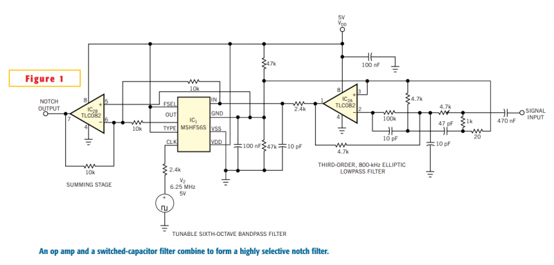
Although you can obtain universal, resistor-programmable switched-capacitor filters that are configurable as notch filters, most cannot operate at bandwidths higher than 100 kHz. Further, the typically 16- to 20-pin packages do not include a continuous-time, antialiasing filter to prevent...
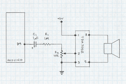
This document demonstrates the use of an Arduino PWM output pin to generate sound. The output pin can be toggled rapidly between LOW and HIGH states to create a square wave. If the frequency of this square wave is...
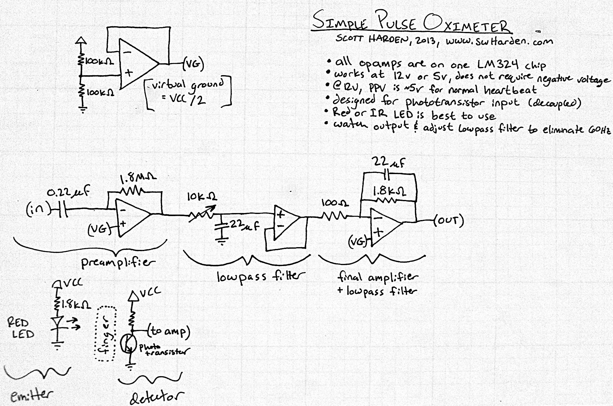
The input capacitor for the phototransistor at the bottom is responsible for feeding the operational amplifier (op-amp). However, the output from the phototransistor consistently remains between ground (GND) and the supply voltage (Vcc). The necessity for an input capacitor...
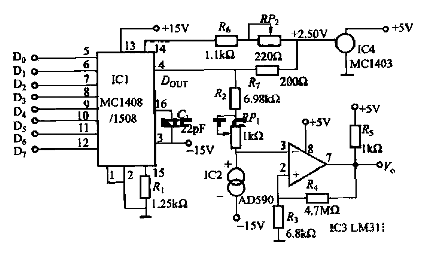
An 8 NC temperature adjusting circuit is presented, primarily composed of a D/A converter, a reference power supply, amplification components, temperature sensors, and other necessary elements. This circuit regulates the temperature within a range of 0-51°C and is suitable...
This circuit diagram illustrates the conversion of a speaker into a microphone. When sound waves impact the diaphragm of a speaker, fluctuations occur in the coil, generating an induced voltage. This induced voltage is typically substantial but low in...
Push-pull outputs are utilized in this transformer-coupled DC-DC regulating converter. It is important to note that the oscillator must be configured to operate at twice the desired output frequency, as the SGI 524's internal flip-flop divides the frequency by...