
Electronic Combination Lock using IC LS 7220
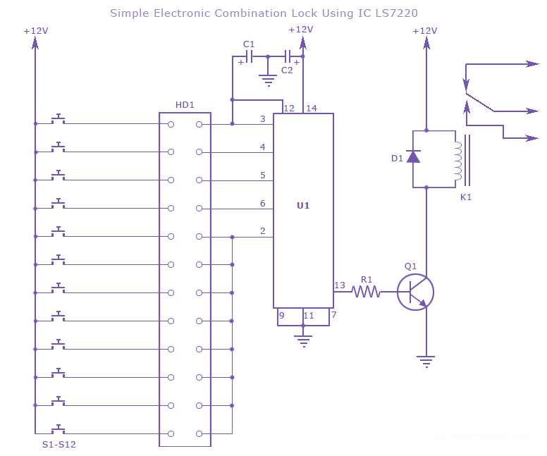
The electronic combination lock circuit employs the LS7220 integrated circuit, which is specifically designed for keypad applications. The circuit's operational voltage range of 5V to 12V allows for versatility in power supply options. The LS7220 facilitates user-defined combinations by connecting switches to its designated input pins. The arrangement of the switches in a 3x4 matrix enables efficient use of space on the PCB while allowing for intuitive user interaction.
When a user inputs the four-digit combination through the connected switches, the LS7220 processes the input. If any incorrect key is pressed during the entry, the circuit resets, ensuring security by requiring the user to start over. This feature is critical in preventing unauthorized access, as it eliminates the possibility of partial inputs being accepted.
The relay output is a key component of the circuit, enabling control over external devices. The duration for which the relay remains activated is determined by the timing capacitor C1. In this design, C1 is set to provide a 6-second activation period, which can be adjusted by changing the capacitor's value. This flexibility allows for customization based on the specific application requirements.
The design also emphasizes user-friendliness, as the keypad layout and labeling can be tailored to the user's preference. The choice to use symbols instead of numbers adds an additional layer of complexity for potential intruders, enhancing security. Overall, this combination lock circuit is a practical and effective solution for secure access control in various applications.This is the circuit diagram of a simple electronic combination lock using IC LS 7220. This circuit can be used to activate a relay for controlling (on & off) any device when a preset combination of 4 digits are pressed. The circuit can be operated from 5V to 12V. To set the combination connect the appropriate switches to pin 3, 4, 5 and 6 of the IC th rough the header. As an example if S1 is connected to pin 3, S2 to pin 4, S3 to pin 5, S4 to pin 6 of the IC, the combination will be 1234. This way we can create any 4 digit combinations. Then connect the rest of the switches to pin 2 of IC. This will cause the IC to reset if any invalid key is pressed, and entire key code has to be re entered.
When the correct key combination is pressed the out put ( relay) will be activated for a preset time determined by the capacitor C1. Here it is set to be 6S. Increase C1 to increase on time. For the key pad, arrange switches in a 3X4 matrix on a PCB. Write the digits on the keys using a marker. Instead of using numbers I wrote some symbols!. The bad guys will be more confused by this. 🔗 External reference
Related Circuits
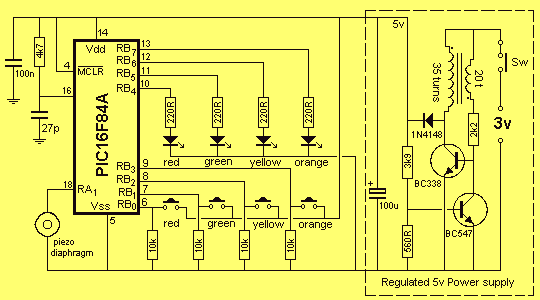
The PC board has been designed to accept either a PIC16F84A or PIC16F628. With the introduction of the 628 to the world market, it has taken over from the PIC16F84A and we will be ceasing to design projects for...
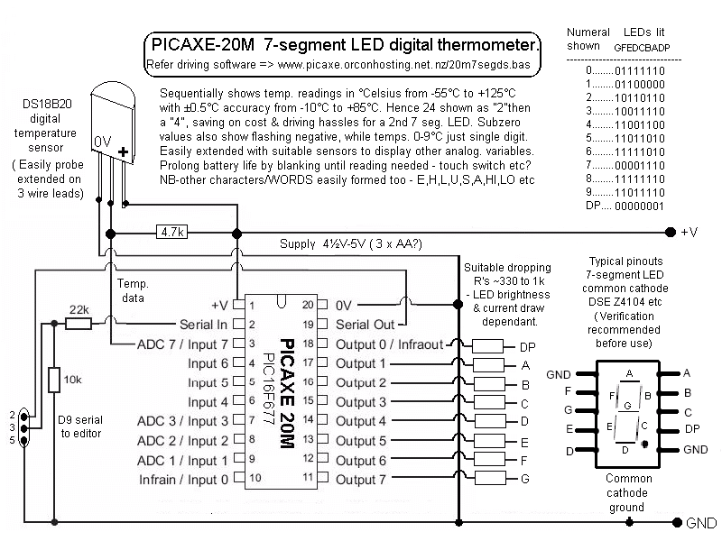
After working with an LCD, driving LED segments becomes relatively straightforward, so programming should not be a major concern. The 20M circuit mentioned earlier includes code and a schematic. The forum receives various educational inquiries, especially close to submission...
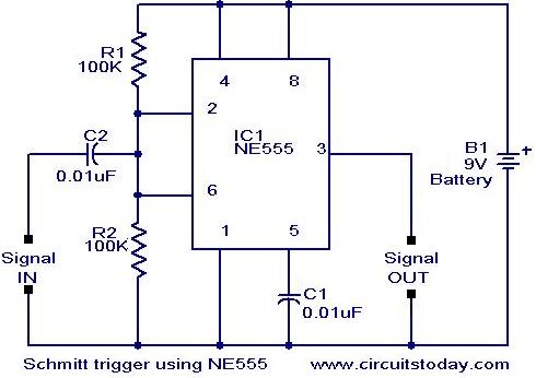
In addition to its timing functions, the two comparators of the 555 timer can be utilized independently for various applications. One such application is a Schmitt Trigger. The inputs of the two comparators (pin 2 and pin 6) are...
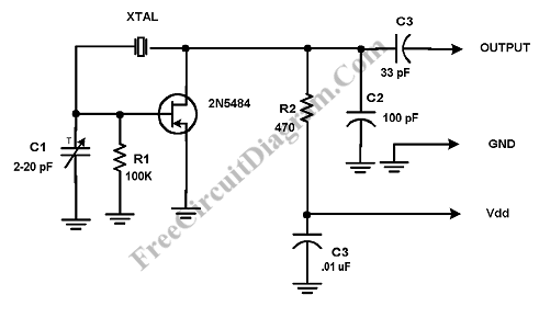
This circuit is a conventional Pierce type oscillator that utilizes a JFET. It employs fundamental mode crystals and demonstrates decent performance and reliability. The Pierce oscillator is a popular configuration for generating stable oscillations, particularly in applications requiring a stable...
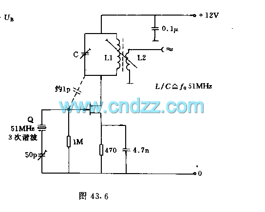
A crystal oscillator operates at a frequency of 51 MHz, which corresponds to the third harmonic of a 17 MHz fundamental frequency. Depending on the specific structure used, the drain-gate capacitance can be selected within a range of 0.5...
This simple and cost-effective ding-dong electronic doorbell circuit is based on IC 8021-2. The IC has an integrated circuitry that generates a ding-dong sound each time its pin 3 is pulled low. The sound is stored in the IC...