
Exit Delay For Burglar Alarms Circuit
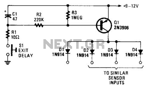
The circuit operates by utilizing a capacitor (CI) that charges to the supply voltage when switch SI is depressed. This action effectively biases transistor Q1 on, facilitated by bias resistors R2 and R3, which are configured to provide the necessary base current to Q1. The charging of CI creates a voltage that remains present throughout the delay period, which serves to temporarily disable the alarm circuit, preventing it from triggering during this designated time frame.
The delay time can be adjusted by modifying the value of capacitor CI. Increasing the capacitance will result in a longer delay, as it takes more time to charge to the supply voltage. Conversely, decreasing the capacitance will shorten the delay time, allowing the alarm circuit to activate more quickly after SI is released. This flexibility in timing is essential for applications where precise control over alarm activation is required.
Resistors R2 and R3 play a crucial role in determining the biasing conditions for transistor Q1. The values of these resistors can also be adjusted to fine-tune the biasing level, impacting the overall response time of the circuit. Proper selection of these components ensures that the transistor operates within its optimal range, thus maintaining reliability and efficiency in the circuit's performance.
In summary, this circuit design allows for adjustable delay times through the manipulation of capacitor CI and the biasing resistors, facilitating effective control over the alarm system's activation. Depressing SI charges CI to the supply voltage. This biases Ql on via bias resistors R2 and R3. A voltage is available for the duration of the delay period, to hold off the alarm circuit. CI can be increased or dccrcascd in value to alter the delay times. 🔗 External reference
Related Circuits
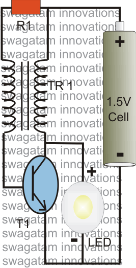
The post explains a simple 1 watt LED driver circuit using a single 1.5 V penlight cell through the joule thief concept. The coil may be wound over a T13 toroidal ferrite core using 0.2 mm or 0.3 mm...
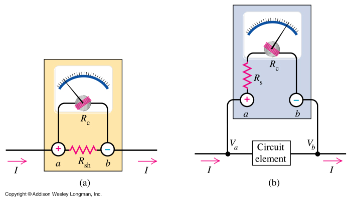
Electron trajectories in a conductor are depicted in the diagrams below. When no electric field is present inside a conducting material, electrons move randomly. However, when an electric field is applied, the electric force F = qE induces a...

This is a simple circuit design for a video transmitter capable of radiating signals up to 50 meters. The video transmitter can be connected to a camera as a source and allows viewing on a VHF channel analog television....
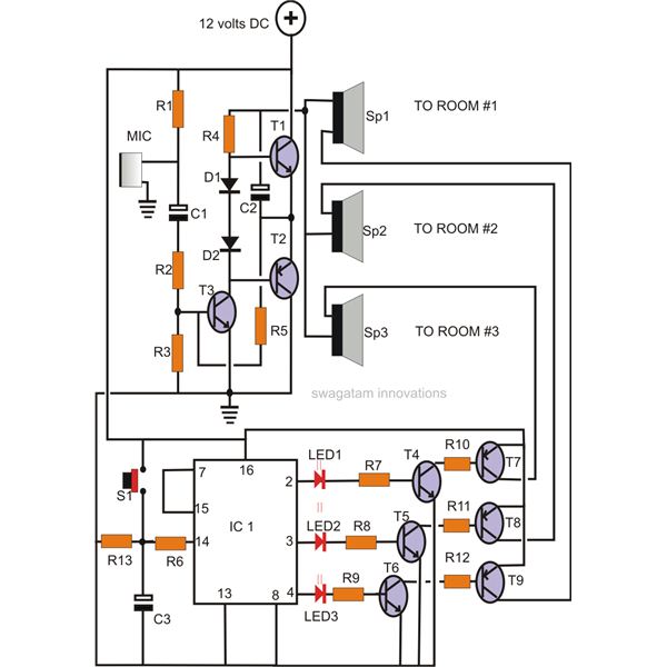
A home intercom system can be constructed using a versatile circuit design. This system allows communication across up to ten different locations or rooms discreetly. It utilizes a single changeover switch for selecting the desired location, replacing the traditional...
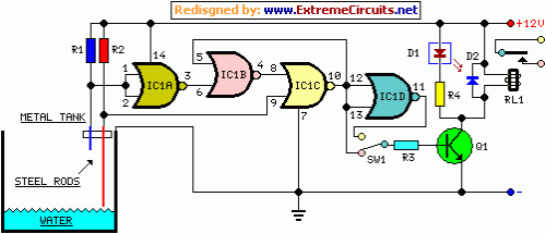
This circuit utilizes a relay to control a water pump, enabling automatic level control for a water reservoir or well. The shorter steel rod acts as the "water high" sensor, while the longer rod serves as the "water low"...
This circuit design for a high-frequency waveform generator is highly beneficial for electronic experiments and designs. The circuit generates sine wave oscillations, but it can also be modified to produce triangle or square wave functions. The high-frequency waveform generator circuit...