
Expressive Arduino Midi Sequencer

The note values are represented in an array: char* intToNote[] = {"C0", "C#0", "D0", "Eb0", "E0", "F0", "F#0", "G0", "G#0", "A0", "Bb0", "B0", "C1", "C#1", "D1", "Eb1", "E1", "F1", "F#1", "G1", "G#1", "A1", "Bb1", "B1", "C2", "C#2", "D2", "Eb2", "E2", "F2", "F#2", "G2", "G#2", "A2", "Bb2", "B2", "C3", "C#3", "D3", "Eb3", "E3", "F3", "F#3", "G3", "G#3", "A3", "Bb3", "B3", "C6", "C#6", "D6", "Eb6", "E6", "F6", "F#6", "G6", "G#6", "A6", "Bb6", "B6", "C7", "C#7", "D7", "Eb7", "E7", "F7", "F#7", "G7", "G#7", "A7", "Bb7", "B7", "C8", "C#8", "D8", "Eb8", "E8", "F8", "F#8", "G8", "G#8", "A8", "Bb8", "B8", "C9", "C#9", "D9", "Eb9", "E9", "F9", "F#9", "G9", "G#9", "A9", "Bb9", "B9"};
The sequencer's operation relies on a systematic approach to address the multiplexers and manage the timing of note playback. The use of a 4-bit binary address allows for precise control over which potentiometer is read at any given moment, ensuring accurate note generation. The sequencer effectively integrates both hardware and software components to create a cohesive musical output. The design utilizes analog multiplexers to handle multiple input signals while maintaining synchronization with the program's execution flow. The implementation of the assignByteToPins function is critical for ensuring that the correct binary address is sent to the multiplexers, allowing for a seamless transition between different notes and velocities. The chosen method of directly manipulating pin states ensures reliability in the signal sent to the multiplexers, thus enhancing the overall performance of the sequencer.This section of code outlines the main sequence of operation for the sequencer. First, a for loop is utilized to govern which step the sequencer is operating in. Within this loop, first an address is made using the assignByteToPins() function, this sends a 4 bit binary address to ensure that the input of each analog multiplexer corresponds to the value of k (the indexing variable of the for loop). Next, an array called "note[]` is assigned a value at position k based on the analog voltage present on pin A0, this is done in a similar fashion for the velocity[] array. Once a value is stored in each array, it is then sent to the computer through USB using the usbMIDI class and the sendNoteOn(note, velocity, channel) function.
Note length and tempo are then determined using either the delay() function or the lengthWait() function to stall the operation of the program for a period of milliseconds. During operation of the sequencer, it is imperative that the desired note is played at any given time.
This is accomplished by making certain that each potentiometer (the input device used to vary a note) is read at the precise time that particular note is to be played. A device known as a multiplexer is used to do this (more information on the multiplexers can be seen in the hardware section).
The inputs are synced to the flow of the program by sending a 4 bit binary address to the multiplexers using the assignByteToPins function. This function takes an integer and based on its value (as long as it is between 0 and 15) will assign the corresponding binary value to the state of digital I/O pins 4 through 7.
This is done by a simple if, if else ladder. While this can be accomplished more elegantly through the use of a for loop and some modulus division, it was found that writing all four pins simultaneously ensures that the desired address is sent to the multiplexer rather than a transient binary value. If a loop based function was used for instance, as the function re assigned states to each of the pins, it would change their values sequentially, and therefore effectively send multiple address signals before settling on a final state.
In the case of switching between binary 7 and binary 8, the sequence in which the pins change state would be as follows; 0111 -> 1110 -> 1100 -> 1000. char* intToNote[] = {"C0", "C#0", "D0", "Eb0", "E0", "F0", "F#0", "G0", "G#0", "A0", "Bb0", "B0", "C1", "C#1", "D1", "Eb1", "E1", "F1", "F#1", "G1", "G#1", "A1", "Bb1", "B1", "C2", "C#2", "D2", "Eb2", "E2", "F2", "F#2", "G2", "G#2", "A2", "Bb2", "B2", "C3", "C#3", "D3", "Eb3", "E3", "F3", "F#3", "G3", "G#3", "A3", "Bb3", "B3", "C6", "C#6", "D6", "Eb6", "E6", "F6", "F#6", "G6", "G#6", "A6", "Bb6", "B6", "C7", "C#7", "D7", "Eb7", "E7", "F7", "F#7", "G7", "G#7", "A7", "Bb7", "B7", "C8", "C#8", "D8", "Eb8", "E8", "F8", "F#8", "G8", "G#8", "A8", "Bb8", "B8", "C9", "C#9", "D9", "Eb9", "E9", "F9", "F#9", "G9", "G#9", "A9", "Bb9", "B9"};
🔗 External reference
Related Circuits
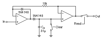
Simplified Analog Input Schematic This schematic represents the input circuitry for a single input. This circuit is a track and hold. The idea is that the input waveform may reach a peak at any instant as the drummer strikes...
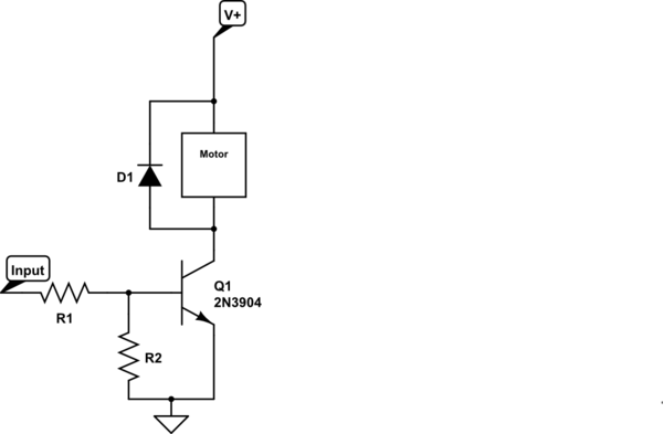
Control a small 5V motor using an external power supply by triggering a transistor with an Arduino. The transistor in use is an NPN type, specifically the 2N3904. To control a small 5V motor using an Arduino and an NPN...
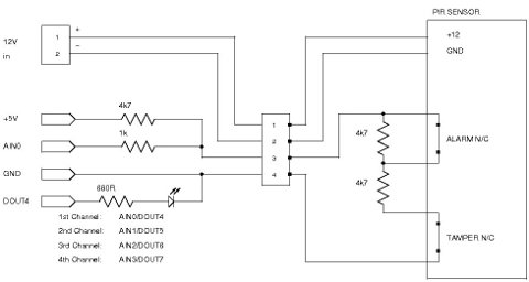
Security system sensors such as motion detectors, reed switches, pressure mats, glass-break detectors, infrared beams, and conductive film can be very useful for various applications, including home automation systems, interactive art installations, and security systems. Almost all security system...
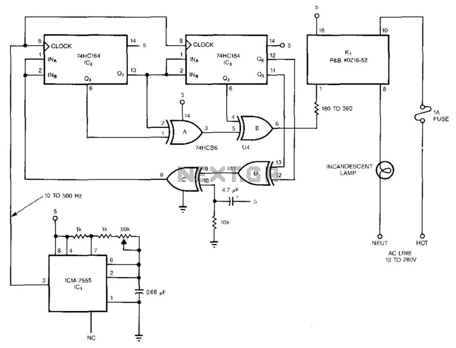
The pseudorandom sequencer drives a solid-state relay. When a low-wattage lamp is powered from the relay, the lamp will flicker like a candle's flame in the wind. Using higher-wattage lamps allows for the simulation of a fireplace or campfire...
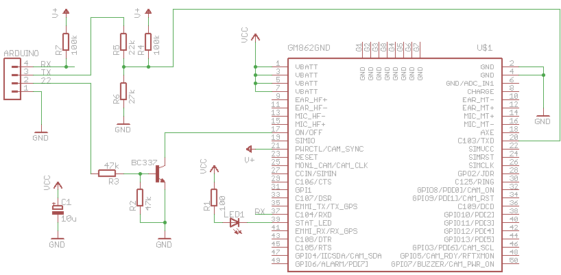
The Arduino can communicate over various networks, including Ethernet, Bluetooth, Wi-Fi, XBEE, and GPRS. A Telit GM862-GPS module, which has GPRS and GPS capabilities accessible via AT commands, has been repurposed for use with the Arduino. The GM862's logic...
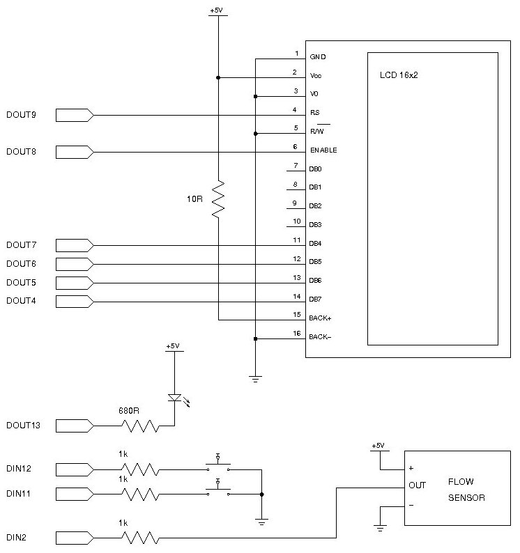
Measuring the consumption of a resource that has units by volume can be more challenging than it appears. Resources such as water, gas, and electricity are typically measured using gauges that determine either the instantaneous flow rate or the...