
Fast Binary Adding Circuits
The Daniels Adder presents a significant advancement in digital circuit design, particularly in binary addition processes. By eliminating carry bits, it simplifies the addition operation, allowing for more efficient circuit implementations. The reliance on recognition patterns enhances the speed and reliability of the addition process, as it aligns closely with the fundamental principles of binary arithmetic.
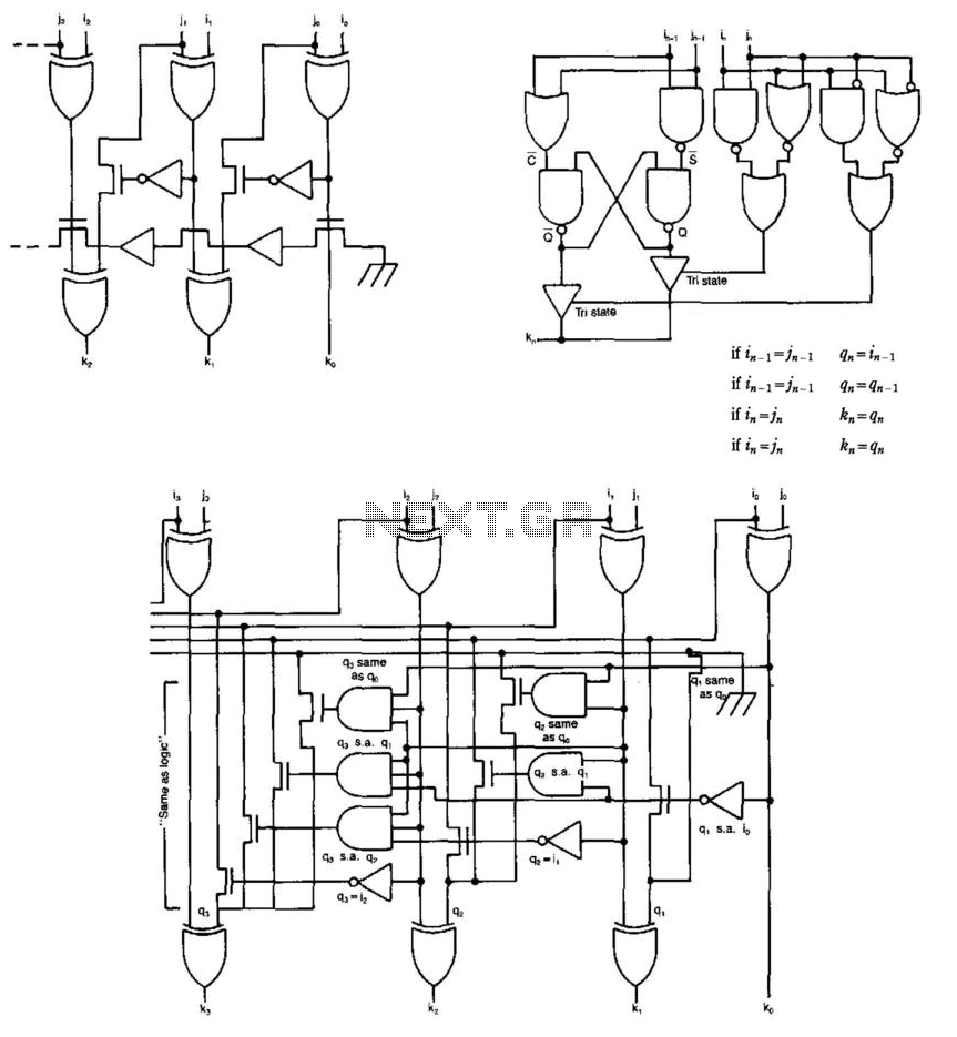
The logic diagram in Figure 45-1 (a) showcases the ripple-through implementation, where each stage operates independently yet simultaneously. This parallel processing capability is critical in achieving high-speed performance. The intermediate variable qn acts as a critical component in determining the output of each stage, allowing the circuit to quickly ascertain whether the current addition operation aligns with the previous stage's result.
In terms of scalability, the architecture of the Daniels Adder supports expansion beyond 4 bits without the complications introduced by traditional carry look-ahead adders. This characteristic is particularly advantageous in applications requiring large-scale binary addition, such as in digital signal processing or high-performance computing environments.
The pipelined design, as depicted in Figure 45-1 (c), further enhances the performance of the adder by allowing multiple addition operations to occur simultaneously across different pipeline stages. This design not only reduces the overall time required to compute the sum but also maximizes the utilization of available circuit resources.
In conclusion, the Daniels Adder represents a modern solution to the challenges posed by carry propagation in binary addition. Its innovative approach to circuit design not only improves speed and efficiency but also reduces silicon area, making it a valuable addition to the toolkit of electronic engineers engaged in the design of high-performance digital systems. Some circuits that add binary numbers have problems with time delay caused by carry propagation. This has been partially solved by the carry look-ahead adder. However, because of the complexity of this scheme, the carry look-ahead logic usually covers no more than 4 bits, and a ripple carry is implemented between the carry look-ahead blocks. The Daniels Adder avoids these problems by presenting a scheme where carry bits are not used at all in the process of binary addition.
It is based on recognition patterns, which exist with the binary addition truth table. The addition is described by the following two sets of equations: with the boundary condition that q_i = 0, where in, j„, and k)t are the bit of binary weight 2n (nth bit) of the addend, summand, and sum respectively, qn is an intermediate variable and qn is the inverse oiqn. The value of the sum is (depending upon in and ;„) either the same as or the inverse of (depending upon ift- and aO, al, or the inverse of the («-l)th bit of the sum.
Figure 45-1 (a) shows the logic diagram of the ripple through implementation of the adder. Because each stage calculates whether its value of the intermediate variable q„ is the same as the previous stage"s value (g„_i) in parallel, it is possible to devise simple "same as" logic that does not have the complexity drawback of carry look-ahead logic and can be carried over any number of bits (Fig. 45-1 (b)). A 32-bit adder built in this way will result in 11-gate delays (no gate having more than 4 inputs). Especially compact and efficient is the pipelined implementation (Fig. 45-1 (c)), which can produce the sum at a rate of 3-gate delays/bit. The high-speed adder circuits can be used on gate arrays or full-custom ICs to implement fast calculation of addresses or data values.
Because of their compact nature, they also use less space on the silicon than conventional adders do. 🔗 External reference
Related Circuits
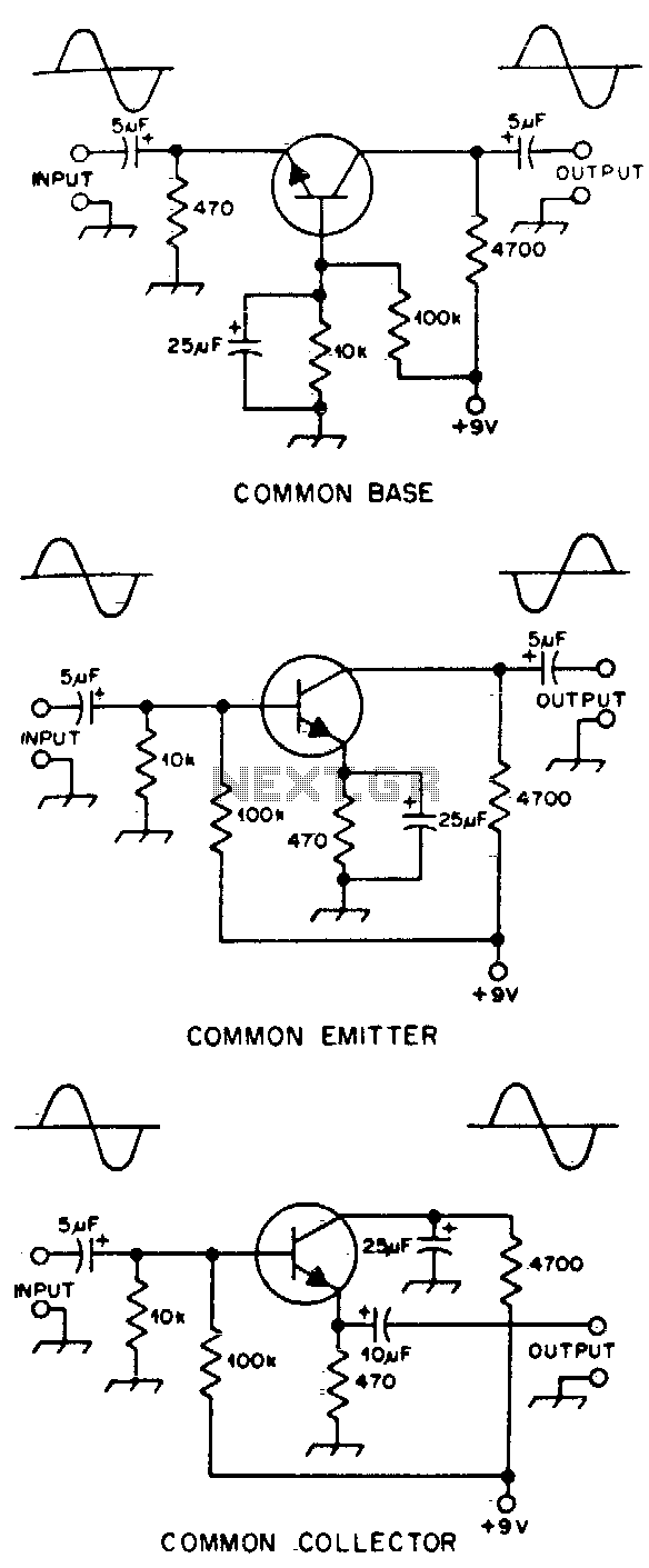
Typical component values are provided for use at audio frequencies, where these circuits are most commonly utilized. The input and output phase relationships are illustrated. The circuit design focuses on audio frequency applications, emphasizing the selection of component values that...
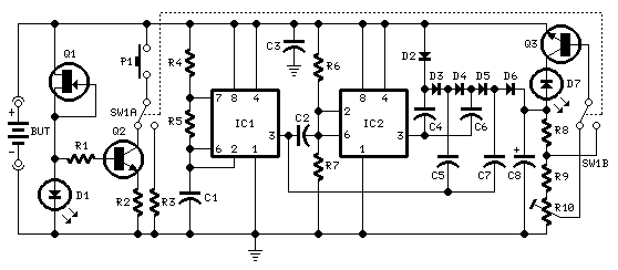
This circuit performs a rapid battery test without requiring an external power supply or costly moving-coil voltmeters. It features two ranges: when switch SW1 is set as indicated in the circuit diagram, the device can test batteries ranging from...
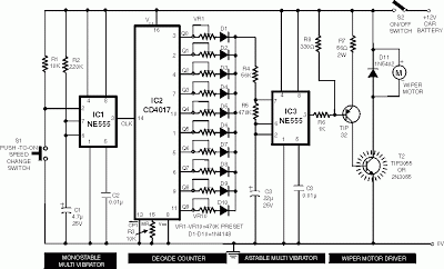
The circuit includes a momentary switch S1 that triggers an alarm pulse for the decade counter IC2, which increments its count with each alternating alarm pulse or the activation of switch S1. Ten variable resistors (VR1 through VR10) are...
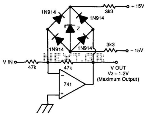
The issue with utilizing two Zener diodes in series for symmetrical clamping is that the knee of the Zener characteristics is imprecise. Additionally, charge storage within the Zeners can lead to speed issues, and the Zeners may exhibit slightly...
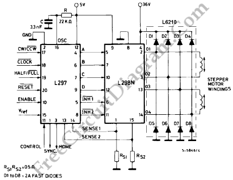
The L29 Stepper Motor Controller IC facilitates the control of four drive signals for two bipolar and four unipolar footfall motors in a microcomputer-controlled appliance. It allows for motor operation in half-step, full-step, and wave drive modes, utilizing switch-mode...
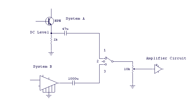
You may be familiar with this effect. You switch audio equipment such as an amplifier to a different input and there is a loud click or "thump" in the speaker system. Not all equipment is affected. Some high-end audio...