
Fast Voltage-Driven Current Source
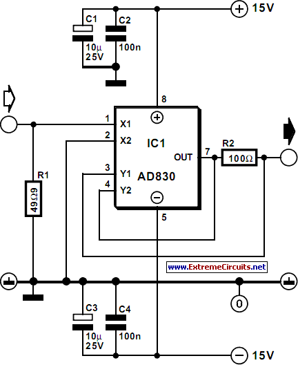
The circuit described involves a current source that is highly responsive to input signal variations, making it suitable for precise measurements in electronic applications. The differential amplifier, designated as IC1, plays a crucial role in maintaining the voltage across resistor R2 at a level that corresponds directly to the input voltage. This relationship is essential for accurate current output, as defined by the equation Iout = Uin/R2, where Uin represents the input voltage.
The bandwidth of the system is a vital parameter, determined by the equation B = R2 f / RL. Here, R2 is the resistance in ohms, f is the frequency set at 80 MHz, and RL is the load impedance, which must be equal to or greater than R2 to ensure optimal performance. The circuit's design incorporates resistor R1, which serves a dual purpose: it provides the necessary 50-ohm termination for compatibility with measurement instruments and establishes the DC operating point of the circuit. In scenarios where the connection to the driving signal source is short and DC-coupled, the inclusion of R1 may be unnecessary, simplifying the circuit design.
To safeguard the integrity of the output current, the circuit limits the peak voltage between pins 1 and 2 of the differential amplifier IC to a maximum of 2.1 V. This limitation is critical in preventing excessive current flow that could potentially damage the circuit components. As a result, the maximum output current is calculated to be 21 mA, derived from the voltage limit divided by the resistance (2.1 V / 100 ohms). This current specification ensures that the circuit operates within safe parameters while providing the necessary response characteristics for high-speed measurements.The current source in the diagram, which react very fast to changes in the input signal, may be used, for instance, in certain measurements. Differential amplifier IC1 ensures that the potential across R2 is equal to the input voltage: Iout =Uin/R2.
The bandwidth, B, is given by B=R2 f /RL, where f=80 MHz, and the load impedance RL‰¥ R2 (both in ohms). The input is terminated into R1 to give the usual 50 impedance required by measuring instruments. At the same time, this resistor sets the d. c. operating point. If the link to the driving signal source is short and d. c. coupled, R1 may be omitted. The peak voltage between pins 1 and 2 of the IC is limited to 2. 1 V to prevent too large a current at the output. Therefore, the peak output current is 2. 1/100=21 mA. 🔗 External reference
Related Circuits
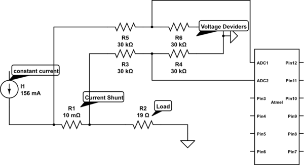
Measure current on a constant current source (LM317). Since a 3.3V chip is being used, a voltage divider is also required for reading the current. Will this circuit function correctly, or will it cause issues by attempting to increase...
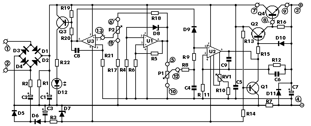
The circuit begins with a step-down mains transformer featuring a secondary winding rated at 24 V/3 A, which connects across the input points at pins 1 and 2. The quality of the output supply is directly related to the...
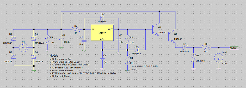
The voltage range will be from 0V to 24V, and the current is not expected to exceed 4A. A microcontroller and an LCD could potentially be added to measure voltage and current. The schematic appears to be generally acceptable....
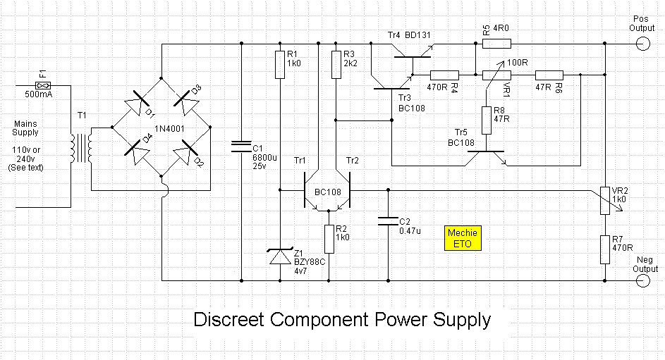
An error amplifier is constructed using transistors Tr1 and Tr2, configured as a differential amplifier, commonly referred to as a long-tailed pair, with the collector leads being a notable feature. One input of this differential amplifier is sourced from...
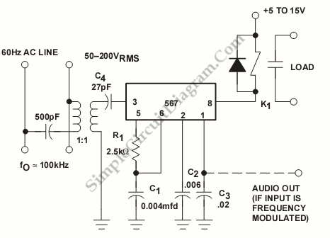
The 567 IC tone decoder/detector can be utilized to construct a remote control or intercom system. This circuit is capable of controlling a relay or transmitting an audio signal. The 567 IC is a versatile component often employed in tone...
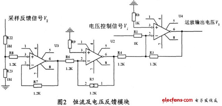
The output current range of the parameter current regulator is limited, and its precision is not high. Connecting the feedback adjustment type output current of the current-stabilized power source in series results in lower efficiency. The steady current source...