
FET biasing
The biasing of FETs, particularly JFETs, is crucial for establishing stable operating conditions in electronic circuits. The self-biasing technique effectively mitigates variations in device characteristics, ensuring that the quiescent point remains stable despite changes in temperature or component tolerances. The use of a voltage divider formed by resistors RG1 and RG2 is a common practice to refine the bias point, allowing for fine-tuning of the gate-source voltage (VGS) to achieve the desired drain current (ID).
In practical applications, the selection of resistor values is vital. The resistors must be chosen to balance the need for stability with the desired operating point. The resistor RG1, which connects the gate to the supply voltage, plays a significant role in adjusting the bias point upward or downward, allowing for greater flexibility in circuit design. Additionally, the source resistor (RS) not only contributes to biasing but also affects the gain and linearity of the amplifier. The value of RS must be carefully calculated to ensure that it does not introduce excessive voltage drop, which could adversely affect the amplifier's performance.
Furthermore, the capacitor (C) in the circuit acts as a coupling element, allowing AC signals to pass while blocking DC. This feature is essential in amplifier applications, where it is critical to isolate the DC operating point from the AC signal variations. The high input impedance of the FET ensures minimal loading on the preceding stage, preserving signal integrity.
In summary, the biasing of FETs, particularly through self-biasing techniques, is essential for ensuring reliable operation in various electronic applications. The careful design of biasing circuits, including the selection of resistors and the incorporation of capacitive coupling, contributes to the overall performance and stability of FET-based amplifiers.Unlike BJTs, thermal runaway does not occur with FETs, as already discussed in our blog. However, the wide differences in maximum and minimum transfer characteristics make ID levels unpredictable with simple fixed-gate bias voltage. To obtain reasonable limits on quiescent drain currents ID and drain-source voltage VDS, source resistor and potenti
al divider bias techniques must be used. With few exceptions, MOSFET bias circuits are similar to those used for JFET s. Various FET biasing circuits are discussed below: DC bias of a FET device needs setting of gate-source voltage VGS to give desired drain current ID. For a JFET drain current is limited by the saturation current IDS. Since the FET has such a high input impedance that no gate current flows and the dc voltage of the gate set by a voltage divider or a fixed battery voltage is not affected or loaded by the FET.
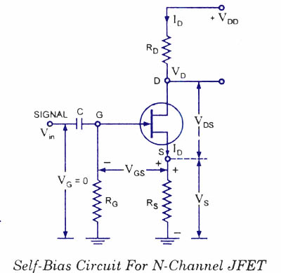
Fixed dc bias is obtained using a battery VQG. This battery ensures that the gate is always negative with respect to source and no current flows through resistor RG and gate terminal that is IG =0. The battery provides a voltage VGS to bias the N-channel JFET, but no resultingcurrent is drawn from the battery VGG.
Resistor RG is included to allow any ac signal applied through capacitor C to develop across RG. While any ac signal will develop across RG, the dc voltage drop across RG is equal to IG RG i. e. 0 volt. So voltage drop across resistance Rs provides thebiasing voltage VGg and no external source is requiredfor biasing and this is the reason that it is called self-biasing. Thus dc conditions of JFET amplifier are fully specified. Self biasing of a JFET stabilizes its quiescent operating point against any change in its parameters like transconductance.
Let the given JFET be replaced by another JFET having the double conductance then drain current will also try to be double but since any increase in voltage drop across Rs, therefore, gate-source voltage, VGS becomes more negative and thus increase in drain current is reduced. A slightly modified form of dc bias is provided by thecircuit shown in figure. The resistors RGl and RG2 form a potential divider across drain supply VDD. The voltage V2 across RG2 provides the necessary bias. The additional gate resistor RGl from gate to supply voltage facilitates in larger adjustment of the dc bias point and permits use of larger valued RS.
🔗 External reference
Related Circuits
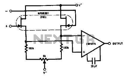
The NPD8301 exhibits excellent characteristics across its range of bias current, enhancing common mode rejection. The monolithic double NPD8301 provides an ideal low offset buffer function and features the LM10lA low drift operational amplifier. The NPD8301 is a monolithic double...
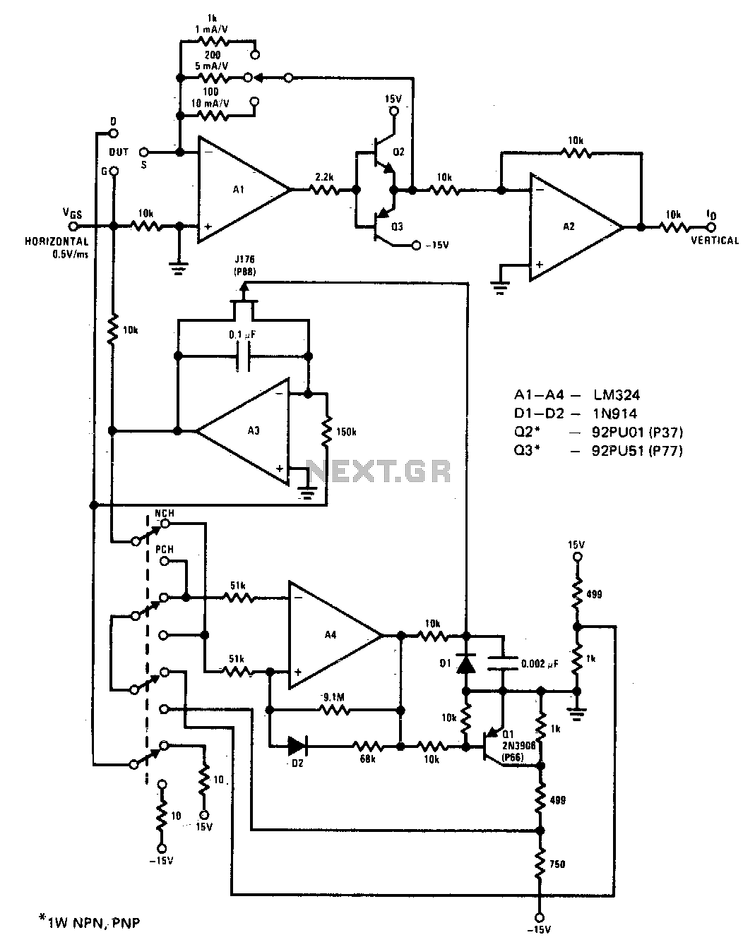
The circuit displays drain current versus gate voltage for both P-channel and N-channel JFETs at a constant drain voltage. The described circuit is designed to analyze the characteristics of Junction Field Effect Transistors (JFETs), specifically focusing on the relationship between...
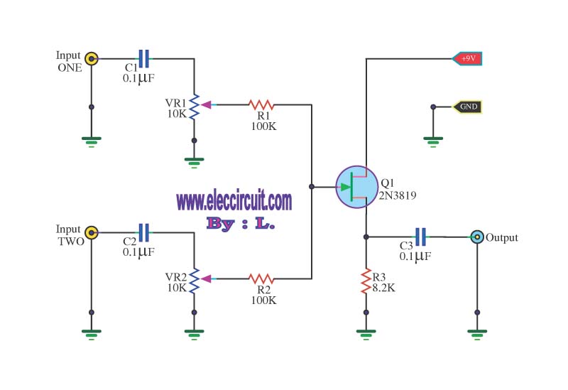
This circuit is a simple mixer circuit that can mix two signal channels into one output channel. It utilizes a codec circuit to convert stereo audio into mono audio. The circuit can also increase the number of channels by...
It employs a low threshold MOSFET and two coupled coils to function as a joule thief. An additional MOSFET is utilized for regulation. The circuit operates as a joule thief, which is a type of DC-DC converter designed to extract...
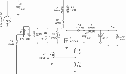
The circuit incorporates components Q, C, and ZD, which are responsible for the bias and buffer stages. Its primary objective is to ensure stable MOSFET gate operation and provide an offset voltage through a voltage buffer amplifier stage with...
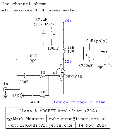
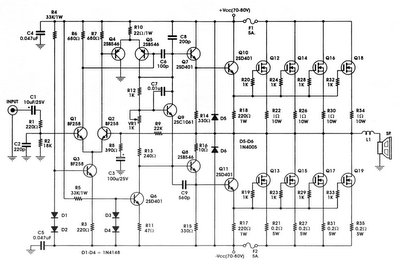
This weblog discusses electronic circuit schematics, PCB design, DIY kits, and electronic project diagrams. It features a simple Class A MOSFET amplifier using the 2SK1058 component. The circuit operates with a 24V supply voltage at high current. It incorporates...