
FFT audio amplifier design
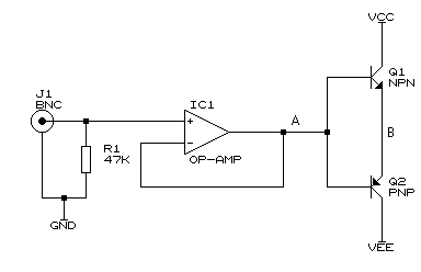
The circuit described utilizes a basic power amplifier with an emitter follower output stage, which is known for its simplicity and effectiveness in driving loads. The emitter follower configuration provides a voltage gain of less than one, making it suitable for applications where a high input impedance and low output impedance are required. The circuit's design allows for easy integration into feedback loops, which is critical for maintaining signal integrity and minimizing distortion.
The initial setup involved connecting the ADC-216 to point A' to monitor the signal quality at the input of the op-amp. The observed performance indicated that the op-amp was functioning well under the influence of negative feedback, yet significant crossover distortion was noted at point B'. This distortion is a common issue in output stages where the transition between the positive and negative halves of the waveform can lead to non-linearities, especially if the output devices are not adequately biased.
To address the distortion, the circuit was modified by introducing a bias voltage between the bases of the output transistors, employing a diode drop technique. This adjustment improved the linearity of the output stage, as evidenced by the nearly 10 dB reduction in THD. The enhanced biasing allows the output devices to conduct more smoothly across the crossover region, thereby reducing the workload on the op-amp to correct for errors.
Furthermore, the use of the PicoScope for spectral analysis provided insight into the harmonic content of the output signal, revealing that the third harmonic was predominant. This information is crucial for diagnosing performance issues in audio applications, where distortion can significantly affect sound quality. The ability to visualize both the time-domain waveform and frequency-domain spectra enables engineers to diagnose and rectify design flaws effectively, leading to improved audio fidelity.
In conclusion, this circuit exemplifies the importance of careful design considerations in amplifier output stages. By utilizing advanced measurement tools and making strategic modifications, significant improvements in performance can be achieved, ultimately resulting in superior sound reproduction.For all of the following tests, we used a high quality signal generator from BlackStar. The PicoScope trace below shows a pure 1 kHz tone from the signal generator. Please note: although the screenshots below show the THD, SFDR and SINAD measurements in a separate window these are now included within the PicoScope program and are displayed in the main window ( see an example ). The diagram below shows a basic power amplifier circuit. The output stage shown is the simple and widely used emitter follower topology. The following tests show how the quality of the signal from output stage can be monitored. Modifications can then be made to the circuit and any improvements recorded. This output stage topology has a stage gain of just less than 1 so it can be easily moved outside the feedback loop as in the circuit below. Initially the circuit was constructed as above. The ADC-216 was connected to point A` in the circuit and the signal generator was connected to the input of the circuit.
The PicoScope screenshot below shows the signal at point A`. It is clear that the op-amp is doing a reasonable job as could be expected with such a large amount of negative feedback applied. If we now look at the output at point B`, we can see excessive crossover distortion clearly visible on the scope trace.
The harmonic information also indicates the problem with the third harmonic component being the largest of the harmonics. The load resistor connected to point B` was 2k2. It is obvious that the output stage is suffering from severe crossover distortion effects. If we continue to monitor point B but move the output stage inside the feedback loop by connecting the inverting input of the opamp to point B`, we notice a massive reduction in the output stage distortion.
Indeed, if you were looking at just the scope trace on a conventional scope, you would not see any problems. This is where the power of the Pico Spectrum Analysis combined with the sensitivity of the ADC-216 are crucial.
The problem is still evident in the spectrum view. If we connect the ADC-216 back to point A` but keep the output stage in the feedback loop, we can see what kind of corrections the opamp is having to apply in order to remove the error generated by the output stage. The opamp follows the sinusoidal signal for the positive and negative peaks of the waveform but around the crossover points, it has to work very hard to cover up the output stage error.
It has to quickly traverse the point where the output stage does not conduct. It is clear then that the opamp needs to have a much higher slew rate, than that which text books may initially suggest, in order to compensate for the poorly designed output stage. This makes the design of earlier gain stages much more difficult and expensive than they need to be. Next the output circuit was improved by applying a bias voltage between the bases of the output devices using the simple diode drop technique.
The view below shows the output at point B` again. It can bee seen that the addition of a small amount of biasing has improved the THD reading by almost 10 dB. If we look again at point A` with this added bias voltage, we can see that the op-amp does not require such a high slew rate since it does not have to work as hard to cover up the output stage imperfections.
This tech note has described a simple application whereby the performance of an amplifier output stage design can be evaluated using the powerful FFT spectrum plot in PicoScope. With some experience, many problems can be identified from their characteristic spectrum plots which might otherwise go unnoticed but lead to a poor or coloured sound reproduction.
🔗 External reference
Related Circuits
This is a four-channel amplifier designed for use with quadraphonic equipment, such as a Sound Blaster Live card. There is no volume control; audio levels are managed directly by the sound card. The construction is straightforward and suitable for...

The following circuit illustrates the BUZ902DP 300 Watt Audio Power Amplifier Circuit Diagram. Features include audio frequency linearity from 20 Hz to 20 kHz. The BUZ902DP is a high-performance audio power amplifier designed to deliver up to 300 watts of...
The amplifier circuit utilizes negative current feedback, which ensures that the load current is primarily influenced by the input signal rather than the loudspeaker's impedance. The inductor current from the loudspeaker generates a voltage across resistor R7, which is...
The following diagram illustrates a common output transformerless (OTL) amplifier circuit that delivers an output power of 100 mW. The circuit includes an output transformer and a capacitor, which work in conjunction with speaker units. The frequency characteristics of...
Create a new project by selecting the New Project option from the Getting Started menu or by selecting File > New Project. This opens a dialog box where the desired project name and location can be entered. Choose a...
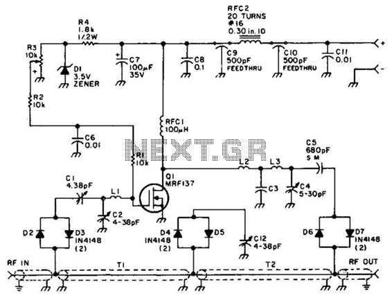
Using a power MOSFET, this amplifier can achieve a 2-W handheld radio power level, increasing it to approximately 10 W on the 2-meter band. A transmission-line RF switch is employed for transmit/receive (T/R) switching. The described amplifier utilizes a power...