
Flight Computer Assembly Instructions
The Flight Computer V1.0 is designed as a versatile and efficient platform for various applications involving microprocessor control. Central to the operation of this flight computer is the U1 80C32 microprocessor, which is known for its low power consumption, making it suitable for battery-operated devices. The microprocessor interfaces with a 32Kx8 ROM (U2 27C256-12) that allows for program storage, and a 32Kx8 RAM (U5 43256-15) for temporary data storage, ensuring efficient operation of the onboard software.
The board's design incorporates multiple supporting components, including a 5V voltage regulator (U4 LM340T-5 or 7805), which provides stable power to the entire circuit. The inclusion of Darlington output transistors (T1-T4 2N6045 or 2N6044) allows for driving larger loads, enhancing the computer's capability to interact with external devices.
Decoupling capacitors (C1-C9) are strategically placed throughout the circuit to ensure stable voltage levels and to filter out noise, thereby improving the reliability of the microprocessor's operation. The crystal oscillator (Y1 11MHz) is crucial for providing the clock signal necessary for the microprocessor's timing, and it can be replaced with alternatives if higher frequencies are required for specific applications.
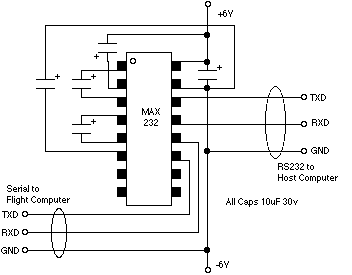
The board features multiple connectors (P1, P2, P3) that facilitate easy integration with other systems, including RS232 communication capabilities via the MAX232 level converter (U100). This allows for straightforward interfacing with computers and other peripherals, making the flight computer adaptable to various control and monitoring tasks.
The printed circuit board (PCB) is double-sided with plated-through holes, allowing for a compact design while ensuring robust electrical connections. The careful design of trace widths and the provision of vias are critical for maintaining signal integrity and managing power distribution across the board.
For assembly, it is essential to follow the guidelines provided to avoid damaging sensitive components. The use of a soldering iron with a fine tip is recommended to minimize heat exposure to the board. Additionally, the ROM is socketed to allow for easy updates and modifications to the firmware, providing flexibility for future enhancements or changes in application requirements.
In summary, the Flight Computer V1.0 serves as a well-engineered solution for those looking to implement microprocessor-based control systems, combining efficiency, adaptability, and user-friendly assembly features.Flight Computer V1. 0: B1 PC Board U1 80C32 microprocessor U2 27C256-12 32Kx8 ROM - 120nS "V2. 1" U3 74HC373 U4 LM340T-5 5v regulator (might be a 7805 part) U5 43256-15 32Kx8 RAM - 150nS U6 74HC00 T1-T4 2N6045 or 2N6044 darlington output transistors Y1 11MHz crystal S1 28-pin socket ROM socket R1 8k2 reset pullup R2 90-120 ohms charge reservoir fill rate R3-R6 10k C1-C2 30 or 33pF C3 10uF C4 100uF power decoupling C5 0. 1uF power decoupling C6 1000uF charge reservoir C7-9 0. 1uF power decoupling P1 6 pin connector main connector P2 10 pin header socket aux connector P3 3 pin header socket serial connector RS232 interface: U100 RS232 level converter - MAX232 or equiv. C100-C104 10uF capacitors P100 RS232 connector for your computer P101 small connector to match P3 above (included in the FC kit) Note that there should also be plugs to match all the connectors on the flight computer and a bag of pins for the plugs - they are very small so be careful you don`t lose them.
P1 is a 0. 156 (really 4mm) pitch molex connector available at many local electronic supply places - P2, P3 are 2mm DF3 connectors by Hirose Electric available from DigiKey. A number of the components - in particular the TO220 transistors and the crystal may have bent leads - straighten them out - they are intended to be placed vertically.
As usual you should observe care with static sensitive parts - only remove them from their tube just prior to using them and always gently ground yourself and your soldering iron tip prior to working with any parts. This board is designed to work with any of the 40-pin 8051/8031/8052/8032 variants of microprocessors - I`ve chosen the 80C32 mostly because it`s available and because it runs at a much lower power than the plain 8051/8031s that are more commonly available (15mA vs 160mA).
The PCB is double sided with plated through holes. It has rather fine traces - take great care not to bridge these use as little solder as you can - too much heat can cause them to lift or damage the thru-holes - try using a soldering iron with the finest tip you can find (1/32 for example) and spend the smallest amount of time possible soldering each pin. Too much heat can cause traces to lift or the plating through to fail (all the holes on the board contain metal that connects the pad on the top with the one under it - many of the small holes you see on the board are `vias` - holes used purely to connect a trace on the top to one on the bottom of the board.
The 11mHz crystal can be replaced with a 12MHz one, or even a 16MHz one (if you have an 80C32-1) - but I`ve used 11MHz because the serial baud rates work out right with the simple timers. In other words the supplied rom will stop working and you will have to provide your own. The ROM is socketed, I`ll provide already burnt ROMs containing a monitor, Basic and Forth that will talk to the serial port at 9600 baud - this monitor only works on 8032/8052 and variants (it uses the upper 128 bytes of on-board SRAM for a buffer).
I`ve tried to write this document so that it has information for people with a whole range of experience building electronic gear - you may find parts of it too wordy - or too difficult or confusing - I`d appreciate feedback to help me make it better. This page is rather long - I wanted to make it easy to print out a copy. Assembly can be done in 1/2 an hour, I suggest you take your time and go as slowly as possible. A component placement diagram is located after the assembly instructions below. Notes: pins on chips are numbered counter clockwise. If you look at the top of a chip (with the pins facing down one end will have a notch or 🔗 External reference
Related Circuits
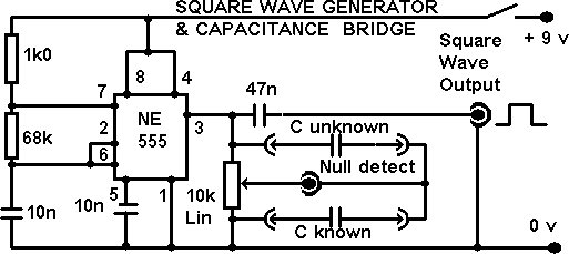
This project integrates multiple features into a compact unit. The core driver is based on an NE555 square wave generator. During development, the idea of building a square wave generator using discrete components was considered, but experiments revealed that...
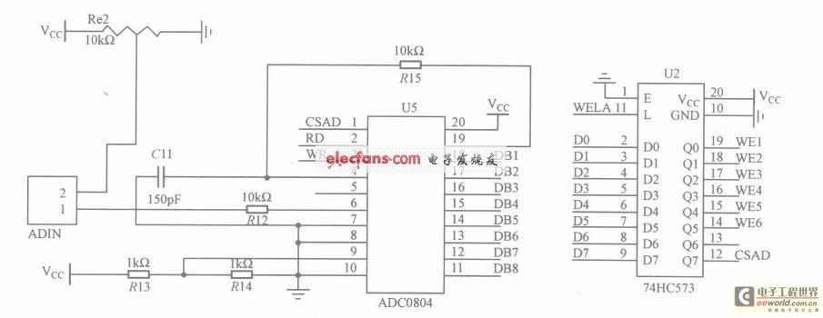
The circuit utilizes the ADC0804, which is configured for left-handed operation, alongside the 74HC573 latch, which is configured for right-handed operation. The latch is connected to a microcontroller, but they are not drawn in the same schematic. The CSAD...
Unplugging or reconnecting devices to the serial COM or PS2 connector can lead to issues if the PC is powered on. This is true even for simple tasks like swapping a mouse or changing from a graphics keyboard to...
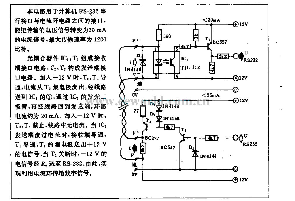
This circuit is utilized in RS-232 serial interface and current loop circuit applications. It converts voltage signals into a 20mA current signal, with a maximum transmission rate of 1200 bits per second. The CCD IC1 and transistor T1 form...
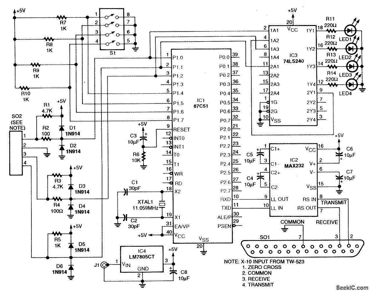
This circuit employs an 87C57 microcontroller along with several peripherals to convert X-10 power-line carrier-code formats from a personal computer for use with an X-10 power-line interface in a home-control system. Software details can be found in the reference. The...
This week, there was a Southern theme in anticipation of Spring Break, leading to the decision to build a LassoBot. This robot throws a lasso in a circular motion until it captures an object in its path. Once an...
Warning: include(partials/cookie-banner.php): Failed to open stream: Permission denied in /var/www/html/nextgr/view-circuit.php on line 713
Warning: include(): Failed opening 'partials/cookie-banner.php' for inclusion (include_path='.:/usr/share/php') in /var/www/html/nextgr/view-circuit.php on line 713