
Assembly of the F&DARC Square Wave Generator/Bridge
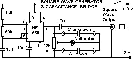
The NE555 square wave generator serves as a versatile component in this project, providing a reliable square wave output that can be utilized in various applications, such as signal generation and testing. The choice of the NE555 timer IC is particularly advantageous due to its well-documented performance and ease of use. The circuit configuration allows for frequency adjustments, enabling users to tailor the output to specific requirements. The integration of a Wheatstone Bridge facilitates capacitance measurements, making the unit suitable for educational and practical applications in electronics.
In the implementation of the circuit, careful attention must be paid to the layout to ensure optimal performance. The use of a PCB is recommended to minimize noise and interference, which can adversely affect the square wave quality. Proper grounding techniques should be employed, and the placement of components should prioritize signal integrity. The calibration process for the potentiometer is crucial for accurate measurements, and users should follow the provided instructions meticulously to achieve reliable results.
Overall, this project not only demonstrates the functionality of the NE555 timer in generating square waves but also showcases the practical application of a Wheatstone Bridge for capacitance measurement, making it a valuable addition to any electronics toolkit.This project combines several features in one compact unit. The fundamental driver consists of a NE 555 square wave generator. During development, consideration and a certain amount of experimentation was given to the construction of a square wave unit using discrete components. Investigation showed however that the geometry of the square wave pro duced was so poor that additional complexity would be needed in the form of a Schmitt trigger circuit. In order to keep the unit as simple as possible, and at the same time produce a usefully clean and symmetrical square wave which could have further applications, the discrete approach was abandoned.
The final square wave generator using an NE555 IC has both a low component count and is simple to construct; it produces an excellent square wave, rich in harmonics (for signal tracing), and ample output to drive the capacitance bridge. The whole unit in its basic form can be constructed on a piece of PCB only three inches square. If a capacitance substitution box - which in itself also has further application - is added, to extend the range and convenience of the bridge, the entire unit occupies 3" x 6".
The unit is powered by a 9 volt PP3 battery. The following instructions include the circuit, component list, comprehensive layout and connection diagrams, and photographs of the completed prototype (basic) unit. The circuit diagram is given in Fig. 1, and is of the project in its basic form, i. e. without the capacitor substitution box. The circuit of the capacitor substitution box is shown in Fig. 2. With the the values of resistors used, this circuit oscillates at about 1 kHz, producing a square wave of approximately equal mark / space ratio.
Should it be necessary at a later date, the frequency may be altered between about 650 Hz and 7. 2 kHz by altering the value of the 68k resistor between 10k and 160k. The range may be further extended by altering the value of the 10nF capacitor on pin 6 of the IC. The mark / space ratio may be altered by changing the ratio of values of the two resistors, although the 1k resistor controls the circuit`s current consumption, and should not be further reduced. The bridge circuit attached to pin 3 of the IC is a conventional Wheatstone Bridge arrangement. The Wheatstone Bridge basic circuit is shown in Fig. 3: with a signal source applied across the two arms of the bridge as shown, and either headphones or other null detector (such as the F&DARC audio amplifier / speaker project) connected across the bridge output, a null (minimum sound) will be heard when the ratio of the resistances is equivalent to the ratio of the capacitances, or R1 / R2 = C1 / C2.
In the circuit of this project, R1 and R2 are replaced by a potentiometer; if C2 is a known value, the potentiometer control may be calibrated in terms of the ratio of the unknown to the known capacitors. Calibration instructions are included at the end of this article. The basic unit as shown in Fig. 1 can be constructed on a 3" square piece of PCB. The complete suggested layout diagram, including the optional capacitance substitution box, is shown in Fig.
4, and needs a 3" x 6" piece of PCB. The square wave generator circuit wiring in the vicinity of the IC is shown in Fig. 5. This, and the photographs should help to clarify the recommended layout. A pin-out diagram for the NE 555 IC is given in Fig. 6. Note that this diagram shows the IC sitting on its pins, whereas the suggested layout uses the chip on its back (dead bug construction). Complete the physical construction before wiring the IC: drill the bare board to accommodate the potentiometer, sockets, switches and choc blocks.
Whilst the layout isn`t critical, be sure to position the components so there`s room to wire everything up, and especially so that there`s room for the battery. In the layout diagrams, the light lines are construction lines, marking the board centre lines and d 🔗 External reference
Related Circuits
One unit is in good condition, manufactured in 1979, and is capable of generating sine, triangle, and square waveforms. This unit is retained and utilized as the primary function generator for testing purposes at the main office location. The...
A 555 timer operating in astable mode generates driving pulses, while two 4518 dual BCD (binary coded decimal) counters provide square waves. A TL081 operational amplifier functions as an output buffer-amplifier. Potentiometers R1 and R2 are utilized to control...
With the advancement of technology and the widespread use of large high-accuracy dynamic range D/A converters for full-speed digital signal processing, the generated frequency remains relatively fixed due to the phase control achieved through digital means and adjustable synthesis...
Frequencies that exceed the limits of human hearing are referred to as ultrasonic waves or frequencies. These ultrasonic waves can be generated using various components, including piezoelectric cells, magnetostrictive oscillators, piezoelectric oscillators, and Hartley oscillators with piezoelectric cells. Ultrasonic waves...
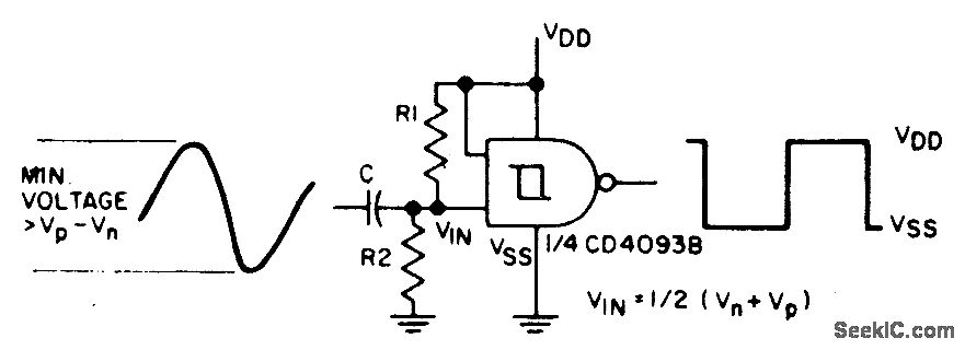
The sine input is AC coupled by capacitor C. Resistors R1 and R2 bias the input midway between Vn and Vp, the input threshold voltages, to provide a square wave at the output. The circuit described utilizes an AC coupling...
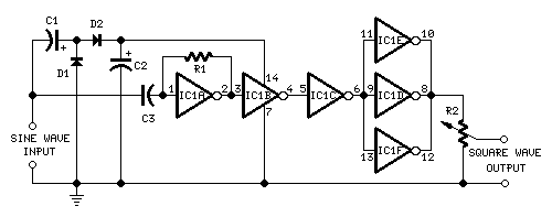
This circuit is intended to provide good square waves converting a sine wave picked up from an existing generator. Its main feature consists in the fact that no power source is needed: thus it can be simply connected between...
Warning: include(partials/cookie-banner.php): Failed to open stream: Permission denied in /var/www/html/nextgr/view-circuit.php on line 713
Warning: include(): Failed opening 'partials/cookie-banner.php' for inclusion (include_path='.:/usr/share/php') in /var/www/html/nextgr/view-circuit.php on line 713