
Floating 9V Supply For DVM Modules With LMC555 IC
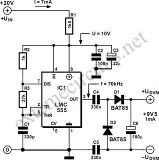
The LMC555 timer IC is a versatile component that can be configured in several modes, including astable, monostable, and bistable operations. In the context of laboratory power supplies, the LMC555 can be utilized to generate precise timing signals or to control the output voltage and current levels.
In an astable configuration, the LMC555 operates as an oscillator, producing a continuous square wave output. This is achieved by connecting resistors and capacitors to the timing pins of the IC, which determine the frequency and duty cycle of the output waveform. The output can be used to drive other circuits or components, such as transistors or relays, to control power delivery.
In monostable mode, the LMC555 can be triggered by an external signal to produce a single pulse of a defined duration. This feature is particularly useful in applications requiring precise timing for triggering events, such as activating relays or switching power supplies on and off.
The LMC555's ability to operate over a wide voltage range and its low power consumption make it suitable for battery-powered devices and portable test equipment. Additionally, the IC's internal circuitry is designed to withstand a range of environmental conditions, enhancing its reliability in laboratory settings.
Overall, the LMC555 timer IC's flexibility and ease of use make it an essential component in the design of laboratory power supplies and test equipment, allowing for accurate control and measurement of electrical parameters.This circuit built from the ubiquitous LMC555 timer IC. Are typically used in laboratory power supplies and other test and measurement equipment .. 🔗 External reference
Related Circuits
A switching power supply with an output voltage significantly lower than its input voltage exhibits an interesting characteristic: the current drawn by the supply is less than its output current. However, the input power (UI) is, of course, greater...
5V regulated power supply circuit, 5V power supply circuit, regulated power supply circuit diagram. The 5V regulated power supply circuit is designed to provide a stable output voltage of 5 volts, which is essential for powering various electronic devices and...
Quasi square wave resonant converters, also referred to as quasi resonant (QR) converters, facilitate the design of flyback Switch Mode Power Supplies (SMPS) with diminished Electro Magnetic Interference (EMI) and enhanced efficiency. Due to their low noise generation, QR...
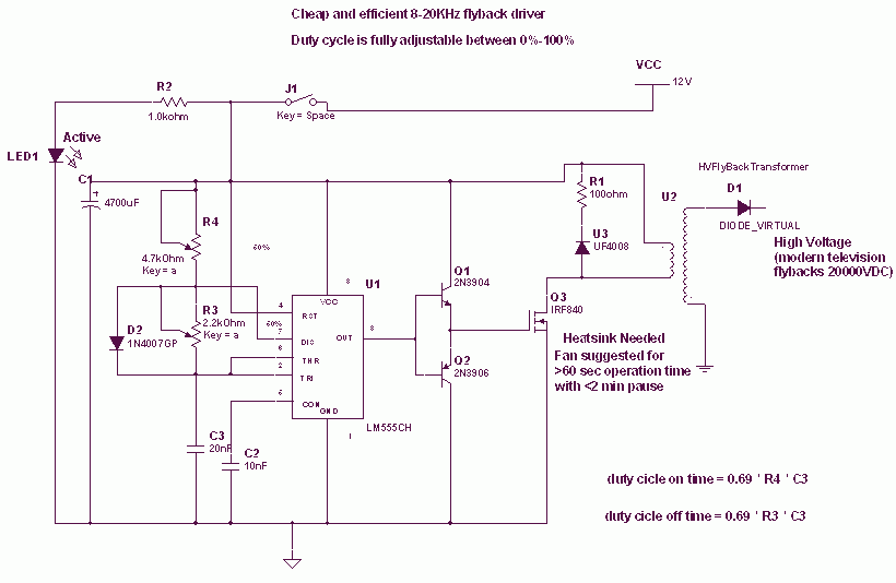
The 555 is wired as an astable and the capacitor is charged only through the 4.7Kohm trimmer (notice the diode) and discharged only through the 2.2 Kohm trimmer, making the duty cycle fully adjustable. The square wave is then...
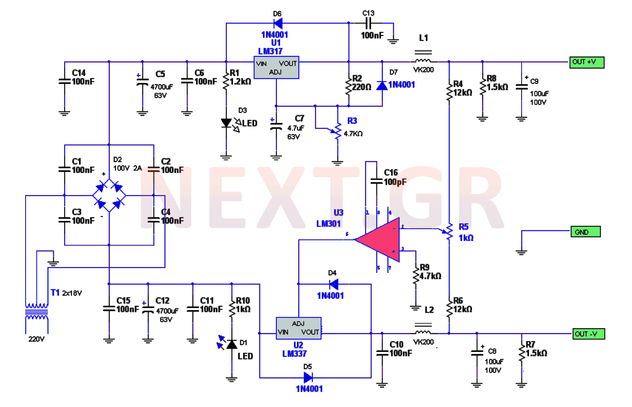
The power supply circuitry includes a 220/2 * 18V / 3.5A transformer, a rectifier, a smoothing filter, a power amplifier (LM301), and two regulators (LM317 and LM337). The voltage from the transformer is rectified by a bridge rectifier. Capacitors...
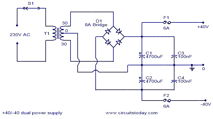
This 40V dual power supply circuit was designed to power a 150 Watt amplifier circuit. The transformer T1 steps down the mains voltage, while bridge D1 performs rectification. Capacitors C1 and C2 act as filters, and C3 and C4...