
fm antenna booster circuit diagram
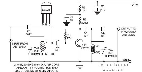
The input coil L1 plays a crucial role in the circuit as it serves to couple the RF signal into the transistor amplifier stage. The use of 20 SWG enamelled copper wire ensures that the coil has a suitable inductance and resistance for effective signal transmission. The slightly spaced winding technique minimizes the capacitance between turns, thereby enhancing the coil's performance at radio frequencies.
Coil L2, with its three turns, functions similarly to L1 but is designed to provide a different inductance value, which can be beneficial for tuning the circuit to specific frequencies or for impedance matching purposes. The reduced number of turns in L2 results in lower inductance, which can be advantageous in certain applications where higher frequency response is required.
The transistor 2SC2570, utilized in this circuit, is a common NPN transistor known for its high frequency and low noise characteristics, making it suitable for RF applications such as FM antenna boosters. The pin configuration of the 2SC2570 is essential for proper integration into the circuit, ensuring that the collector, base, and emitter are correctly connected to optimize the transistor's performance.
Overall, the combination of the two coils and the transistor creates a tuned circuit that can amplify weak RF signals captured by the antenna, significantly improving reception quality. Proper attention to the winding technique, number of turns, and transistor configuration is critical in achieving optimal performance in FM antenna booster applications.Input coil L1 consists of four turns of 20SWG enamelled copper wire (slightly space wound) over 5mm diameter former. It is tapped at the first turn from ground lead side. Coil L2 is similar to L1, but has only three turns. Pin configuration of transistor 2SC2570 is shown in the fm antenna booster schematic. 🔗 External reference
Related Circuits
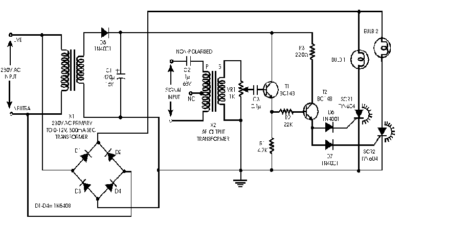
Audio light modulations add to the enjoyment of music during functions organised at home or outdoors. Presented here is one such simple circuit in which light is modulated using a small fraction of the audio output from the speaker...
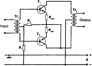
An amplifier is a device that accepts a varying input signal and produces an output signal that varies in the same way as the input but has a larger amplitude. The input signal may be a current, voltage, mechanical...
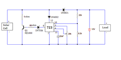
The ultimate source of energy is the Sun. It is possible to generate current from sunlight using solar panels. These panels convert light energy into electrical energy. A solar panel consists of a number of solar cells, which produce...
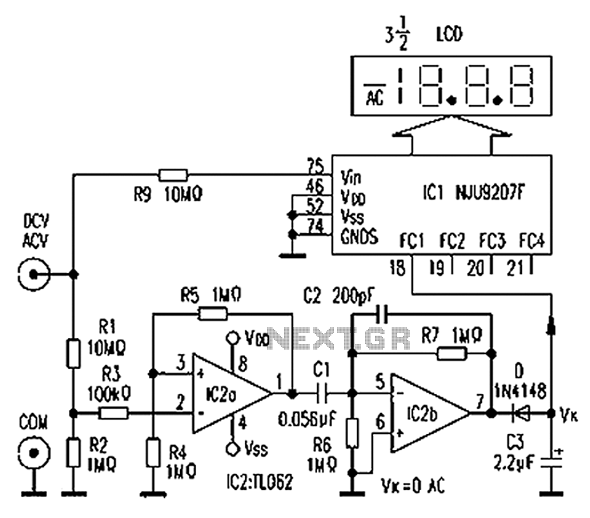
The circuit depicted in the figure illustrates an automatic AC/DC converter for a digital multimeter. Typically, standard digital multimeters require manual intervention to switch between AC and DC measurements. The new DT860D digital multimeter utilizes the NJU9207F automatic range...
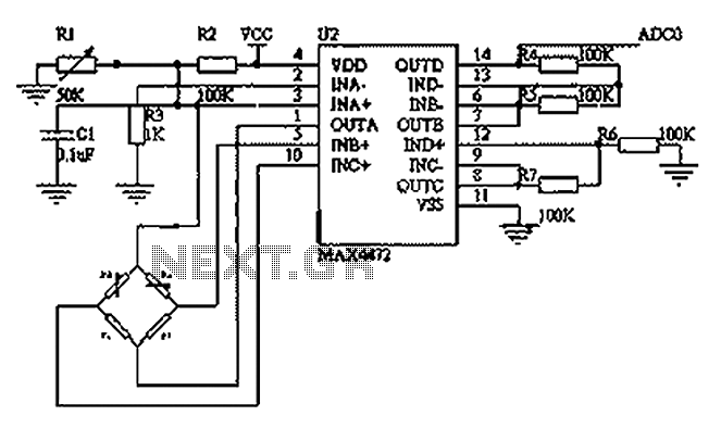
This circuit utilizes a BP01-type pressure sensor and the MAX4472 operational amplifier. The BP01 pressure sensor is specifically designed for blood pressure detection and is primarily used in portable electronic sphygmomanometers. It features a precision thick film ceramic chip...
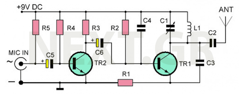
The recommended transmitter is straightforward to construct and suitable for beginners. Despite its simple design and compact size, it delivers remarkable performance. It operates for 12-15 hours on a 9-volt battery and has a transmission range of 100 to...