
FM Jammer Circuit With 2N2222 Transistor
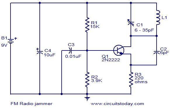
The FM jammer circuit operates by generating a strong VHF (Very High Frequency) signal that disrupts the reception of FM (Frequency Modulation) broadcasts. This is achieved through the use of an oscillator circuit, which is the core component responsible for producing the jamming signal. The oscillator can be based on a variety of configurations, such as a Colpitts or Hartley oscillator, depending on the desired frequency range and stability.
In the typical design, the oscillator circuit is powered by a DC power supply, which could range from a battery to a dedicated power adapter. The output of the oscillator is then amplified using a radio frequency (RF) amplifier to ensure that the jamming signal is strong enough to interfere with the FM signals in the vicinity. The amplified signal is then fed into an antenna, which radiates the jamming signal into the air.
The frequency of the jamming signal is usually set to match or closely overlap with the frequencies of the FM stations in the target area. This overlap is crucial, as it allows the jamming signal to effectively mask the original FM broadcasts, rendering them inaudible to receivers within range.
It is important to note that the use of FM jammers is illegal in many jurisdictions due to their potential to disrupt communication and broadcast services. Regulatory bodies impose strict penalties for unauthorized use of such devices, as they can interfere with emergency services and other critical communications. Therefore, it is essential to consider the legal implications and ethical responsibilities associated with the design and use of FM jamming technology.The Fm jammer circuit diagram transmit VHF signals.Normally powerful oscillation of the circuit interrupt FM signals. Jammers are ban in lots of .. 🔗 External reference
Related Circuits
There was difficulty in understanding that the Source pin connects to low voltage (source of electrons) and the Drain pin connects to high voltage (absorbs electrons). This concept is fundamental to basic electricity, but it required some time to...

the entire circuit is comprised of integrated circuits. This makes for some easy organization when it goes to the circuit board for soldering. In addition, I used only 3 of the pins on the 3rd nixie tube for the...
Locker Guard Circuit Diagram. This compact circuit is designed to protect a locker or almirah from burglary. If the locker is opened while in the armed state, the circuit triggers a loud police siren to deter the burglary attempt. The...
The circuit for a transistor tester is a relatively simple device. The transistor tester circuit illustrated below can be utilized to measure and identify the pins of a transistor, as well as determine its condition. Furthermore, this circuit can...
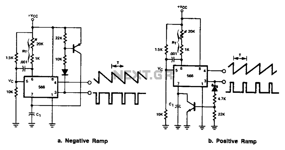
The 566 can be connected to either a positive or negative ramp generator. For a positive ramp generator, an external transistor is driven by the output pin 3. At the end of charging, C1 discharges quickly, allowing for immediate...
A newcomer to the forum is seeking assistance with DIY electronic circuits and lacks a formal background in electrical engineering. The inquiry indicates a desire to learn and engage with the community on topics related to DIY electronic circuits. For...